DDB3. When the pin is forced to be an input, the pull-up can still be controlled by the
PORTB3 bit.
• MOSI – Port B, Bit 2
MOSI, SPI Master Data output, Slave Data input for SPI channel. When the SPI is
enabled as a slave, this pin is configured as an input regardless of the setting of DDB2.
When the SPI is enabled as a master, the data direction of this pin is controlled by
DDB2. When the pin is forced to be an input, the pull-up can still be controlled by the
PORTB2 bit.
• SCK – Port B, Bit 1
SCK, Master Clock output, Slave Clock input pin for SPI channel. When the SPI is
enabled as a slave, this pin is configured as an input regardless of the setting of DDB1.
When the SPI is enabled as a master, the data direction of this pin is controlled by
DDB1. When the pin is forced to be an input, the pull-up can still be controlled by the
PORTB1 bit.
• SS – Port B, Bit 0
SS, Slave Port Select input. When the SPI is enabled as a slave, this pin is configured
as an input regardless of the setting of DDB0. As a slave, the SPI is activated when this
pin is driven low. When the SPI is enabled as a master, the data direction of this pin is
controlled by DDB0. When the pin is forced to be an input, the pull-up can still be con-
trolled by the PORTB0 bit.
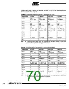
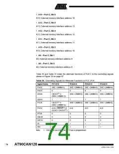
Table 33 and Table 34 relate the alternate functions of Port B to the overriding signals
shown in Figure 34 on page 67. SPI MSTR INPUT and SPI SLAVE OUTPUT constitute
the MISO signal, while MOSI is divided into SPI MSTR OUTPUT and SPI SLAVE
INPUT.
Table 33 and Table 34 relates the alternate functions of Port B to the overriding signals
shown in Figure 34 on page 67.
Table 33. Overriding Signals for Alternate Functions in PB7..PB4
Signal Name
PUOE
PB7/OC0A/OC1C
PB6/OC1B
PB5/OC1A
PB4/OC2A
0
0
0
0
0
0
0
0
0
0
0
0
0
0
0
0
PUOV
DDOE
DDOV
PVOE
OC0A/OC1C
ENABLE(1)
OC1B ENABLE OC1A ENABLE OC2A ENABLE
PVOV
PTOE
DIEOE
DIEOV
DI
OC0A/OC1C(1)
OC1B
OC1A
OC2A
0
0
0
–
–
0
0
0
–
–
0
0
0
–
–
0
0
0
–
–
AIO
Note:
1. See “Output Compare Modulator - OCM” on page 160 for details.
72
AT90CAN128
4250E–CAN–12/04

 ATMEL [ ATMEL ]