AT90CAN128
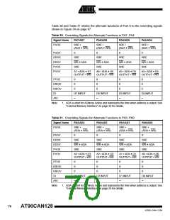
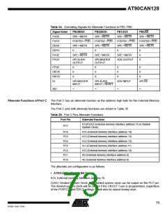
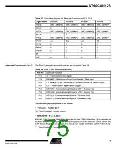
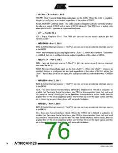
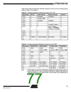
Table 34. Overriding Signals for Alternate Functions in PB3..PB0
Signal Name
PUOE
PB3/MISO
SPE • MSTR
PORTB3 • PUD
SPE • MSTR
0
PB2/MOSI
SPE • MSTR
PORTB2 • PUD
SPE • MSTR
0
PB1/SCK
PB0/SS
SPE • MSTR
PORTB1 • PUD
SPE • MSTR
0
SPE • MSTR
PUOV
PORTB0 • PUD
DDOE
SPE • MSTR
DDOV
0
0
0
PVOE
SPE • MSTR
SPE • MSTR
SPE • MSTR
SCK OUTPUT
PVOV
SPI SLAVE
OUTPUT
SPI MASTER
OUTPUT
PTOE
DIEOE
DIEOV
DI
0
0
0
0
0
0
0
0
0
0
0
0
SPI MASTER
INPUT
SPI SLAVE
INPUT • RESET
SCK INPUT
SPI SS
AIO
–
–
–
–
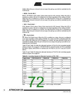
Alternate Functions of Port C The Port C has an alternate function as the address high byte for the External Memory
Interface.
The Port C pins with alternate functions are shown in Table 35.
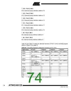
Table 35. Port C Pins Alternate Functions
Port Pin
Alternate Function
A15/CLKO (External memory interface address 15 or Divided
System Clock)
PC7
PC6
PC5
PC4
PC3
PC2
PC1
PC0
A14 (External memory interface address 14)
A13 (External memory interface address 13)
A12 (External memory interface address 12)
A11 (External memory interface address 11)
A10 (External memory interface address 10)
A9 (External memory interface address 9)
A8 (External memory interface address 8)
The alternate pin configuration is as follows:
• A15/CLKO – Port C, Bit 7
A15, External memory interface address 15.
CLKO, Divided System Clock: The divided system clock can be output on the PC7 pin.
The divided system clock will be output if the CKOUT Fuse is programmed, regardless
of the PORTC7 and DDC7 settings. It will also be output during reset.
73
4250E–CAN–12/04

 ATMEL [ ATMEL ]