AT90CAN128
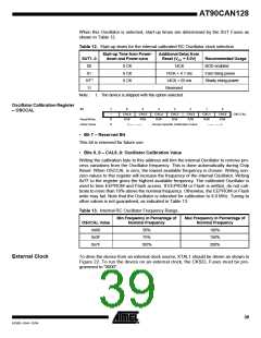
AT90CAN128 share the Timer/Counter2 Oscillator Pins (TOSC1 and TOSC2) with PG4
and PG3. This means that both PG4 and PG3 can only be used when the
Timer/Counter2 Oscillator is not enable.
Applying an external clock source to TOSC1 can be done in asynchronous operation if
EXTCLK in the ASSR Register is written to logic one. See “Asynchronous operation of
the Timer/Counter2” on page 154 for further description on selecting external clock as
input instead of a 32 kHz crystal. In this configuration, PG4 cannot be used but PG3 is
available.
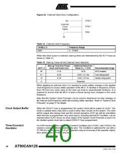
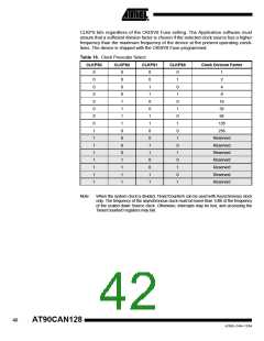
System Clock Prescaler
The AT90CAN128 system clock can be divided by setting the Clock Prescaler Register
– CLKPR. This feature can be used to decrease power consumption when the require-
ment for processing power is low. This can be used with all clock source options, and it
will affect the clock frequency of the CPU and all synchronous peripherals. clkI/O, clkADC
clkCPU, and clkFLASH are divided by a factor as shown in Table 16.
,
Clock Prescaler Register –
CLKPR
Bit
7
CLKPCE
R/W
6
–
5
–
4
–
3
2
1
0
CLKPS3 CLKPS2 CLKPS1 CLKPS0
R/W R/W R/W R/W
See Bit Description
CLKPR
Read/Write
Initial Value
R
0
R
0
R
0
0
• Bit 7 – CLKPCE: Clock Prescaler Change Enable
The CLKPCE bit must be written to logic one to enable change of the CLKPS bits. The
CLKPCE bit is only updated when the other bits in CLKPR are simultaneously written to
zero. CLKPCE is cleared by hardware four cycles after it is written or when CLKPS bits
are written. Rewriting the CLKPCE bit within this time-out period does neither extend the
time-out period, nor clear the CLKPCE bit.
• Bit 6..0 – Reserved Bits
These bits are reserved for future use.
• Bits 3..0 – CLKPS3..0: Clock Prescaler Select Bits 3 - 0
These bits define the division factor between the selected clock source and the internal
system clock. These bits can be written run-time to vary the clock frequency to suit the
application requirements. As the divider divides the master clock input to the MCU, the
speed of all synchronous peripherals is reduced when a division factor is used. The divi-
sion factors are given in Table 16.
To avoid unintentional changes of clock frequency, a special write procedure must be
followed to change the CLKPS bits:
1. Write the Clock Prescaler Change Enable (CLKPCE) bit to one and all other bits
in CLKPR to zero.
2. Within four cycles, write the desired value to CLKPS while writing a zero to
CLKPCE.
Interrupts must be disabled when changing prescaler setting to make sure the write pro-
cedure is not interrupted.
The CKDIV8 Fuse determines the initial value of the CLKPS bits. If CKDIV8 is unpro-
grammed, the CLKPS bits will be reset to “0000”. If CKDIV8 is programmed, CLKPS bits
are reset to “0011”, giving a division factor of 8 at start up. This feature should be used if
the selected clock source has a higher frequency than the maximum frequency of the
device at the present operating conditions. Note that any value can be written to the
41
4250E–CAN–12/04

 ATMEL [ ATMEL ]