AT90CAN128
When this Oscillator is selected, start-up times are determined by the SUT Fuses as
shown in Table 12.
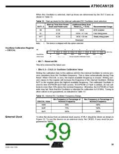
Table 12. Start-up times for the internal calibrated RC Oscillator clock selection
Start-up Time from Power-
down and Power-save
Additional Delay from
Reset (VCC = 5.0V)
SUT1..0
00
Recommended Usage
BOD enabled
6 CK
6 CK
6 CK
14CK
01
14CK + 4.1 ms
14CK + 65 ms
Reserved
Fast rising power
Slowly rising power
10(1)
11
Note:
1. The device is shipped with this option selected.
Oscillator Calibration Register
– OSCCAL
Bit
7
–
6
5
4
3
2
1
0
CAL6
R/W
CAL5
R/W
CAL4
R/W
CAL3
R/W
CAL2
R/W
CAL1
R/W
CAL0
R/W
OSCCAL
Read/Write
Initial Value
R
0
<----- ------
Device Specific Calibration Value
------ ----->
• Bit 7 – Reserved Bit
This bit is reserved for future use.
• Bits 6..0 – CAL6..0: Oscillator Calibration Value
Writing the calibration byte to this address will trim the internal Oscillator to remove pro-
cess variations from the Oscillator frequency. This is done automatically during Chip
Reset. When OSCCAL is zero, the lowest available frequency is chosen. Writing non-
zero values to this register will increase the frequency of the internal Oscillator. Writing
0x7F to the register gives the highest available frequency. The calibrated Oscillator is
used to time EEPROM and Flash access. If EEPROM or Flash is written, do not cali-
brate to more than 10% above the nominal frequency. Otherwise, the EEPROM or Flash
write may fail. Note that the Oscillator is intended for calibration to 8.0 MHz. Tuning to
other values is not guaranteed, as indicated in Table 13.
Table 13. Internal RC Oscillator Frequency Range.
Min Frequency in Percentage of
Nominal Frequency
Max Frequency in Percentage of
Nominal Frequency
OSCCAL Value
0x00
50%
75%
100%
150%
200%
0x3F
0x7F
100%
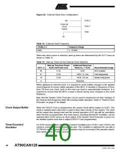
External Clock
To drive the device from an external clock source, XTAL1 should be driven as shown in
Figure 22. To run the device on an external clock, the CKSEL Fuses must be pro-
grammed to “0000”.
39
4250E–CAN–12/04

 ATMEL [ ATMEL ]