AT90CAN128
Timer/Counter2 interrupt enable bits are set in TIMSK2, and the global interrupt enable
bit in SREG is set.
If the Asynchronous Timer is NOT clocked asynchronously, Power-down mode is rec-
ommended instead of Power-save mode because the contents of the registers in the
asynchronous timer should be considered undefined after wake-up in Power-save mode
if AS2 is 0.
This sleep mode basically halts all clocks except clkASY, allowing operation only of asyn-
chronous modules, including Timer/Counter2 if clocked asynchronously.
Standby Mode
When the SM2..0 bits are 110 and an External Crystal/Resonator clock option is
selected, the SLEEP instruction makes the MCU enter Standby mode. This mode is
identical to Power-down with the exception that the Oscillator is kept running. From
Standby mode, the device wakes up in 6 clock cycles.
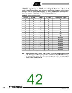
Table 18. Active Clock Domains and Wake-up Sources in the Different Sleep Modes.
Active Clock Domains
Oscillators
Wake-up Sources
Main Clock
Source
Enabled
TWI
Address
Match
SPM/
EEPROM
Ready
TimerOsc
Enabled
Other
I/O
Sleep Mode
clkCPU clkFLASH clkIO clkADC clkASY
INT7:0
Timer2
ADC
Idle
X
X
X
X
X(2)
X
X
X
X
X
X
ADC Noise
Reduction
X
X
X
X(2)
X(3)
X(3)
X(3)
X(3)
X
X
X
X
X(2)
X
X
Power-down
Power-save
Standby(1)
X(2)
X(2)
X(2)
X
Notes: 1. Only recommended with external crystal or resonator selected as clock source.
2. If AS2 bit in ASSR is set.
3. Only INT3:0 or level interrupt INT7:4.
Minimizing Power
Consumption
There are several issues to consider when trying to minimize the power consumption in
an AVR controlled system. In general, sleep modes should be used as much as possi-
ble, and the sleep mode should be selected so that as few as possible of the device’s
functions are operating. All functions not needed should be disabled. In particular, the
following modules may need special consideration when trying to achieve the lowest
possible power consumption.
Analog to Digital Converter
Analog Comparator
If enabled, the ADC will be enabled in all sleep modes. To save power, the ADC should
be disabled before entering any sleep mode. When the ADC is turned off and on again,
the next conversion will be an extended conversion. Refer to “Analog to Digital Con-
verter - ADC” on page 265 for details on ADC operation.
When entering Idle mode, the Analog Comparator should be disabled if not used. When
entering ADC Noise Reduction mode, the Analog Comparator should be disabled. In
other sleep modes, the Analog Comparator is automatically disabled. However, if the
Analog Comparator is set up to use the Internal Voltage Reference as input, the Analog
Comparator should be disabled in all sleep modes. Otherwise, the Internal Voltage Ref-
erence will be enabled, independent of sleep mode. Refer to “Analog Comparator” on
page 262 for details on how to configure the Analog Comparator.
45
4250E–CAN–12/04

 ATMEL [ ATMEL ]