Overview
Many register and bit references in this section are written in general form.
A lower case “n” replaces the USART number, in this case 0 and 1. However, when
using the register or bit defines in a program, the precise form must be used, i.e., UDR0
for accessing USART0 I/O data value and so on.
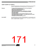
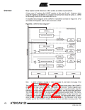
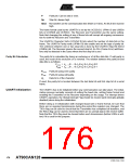
A simplified block diagram of the USARTn Transmitter is shown in Figure 83. CPU
accessible I/O Registers and I/O pins are shown in bold.
Figure 83. USARTn Block Diagram(1)
Clock Generator
UBRRn[H:L]
CLKio
BAUD RATE GENERATOR
SYNC LOGIC
PIN
XCKn
CONTROL
Transmitter
TX
CONTROL
UDRn (Transmit)
PARITY
GENERATOR
PIN
CONTROL
TRANSMIT SHIFT REGISTER
TxDn
Receiver
CLOCK
RX
RECOVERY
CONTROL
DATA
RECOVERY
PIN
CONTROL
RECEIVE SHIFT REGISTER
RxDn
PARITY
CHECKER
UDRn (Receive)
UCSRAn
UCSRBn
UCSRCn
Note:
1. Refer to Figure 2 on page 4, Table 41 on page 78, and Table 36 on page 74 for
USARTn pin placement.
The dashed boxes in the block diagram separate the three main parts of the USARTn
(listed from the top): Clock Generator, Transmitter and Receiver. Control registers are
shared by all units. The Clock Generation logic consists of synchronization logic for
external clock input used by synchronous slave operation, and the baud rate generator.
The XCKn (Transfer Clock) pin is only used by synchronous transfer mode. The Trans-
mitter consists of a single write buffer, a serial Shift Register, Parity Generator and
Control logic for handling different serial frame formats. The write buffer allows a contin-
uous transfer of data without any delay between frames. The Receiver is the most
complex part of the USARTn module due to its clock and data recovery units. The
172
AT90CAN128
4250E–CAN–12/04

 ATMEL [ ATMEL ]