AT90CAN128
• Bit 7 – SPIF: SPI Interrupt Flag
When a serial transfer is complete, the SPIF flag is set. An interrupt is generated if SPIE
in SPCR is set and global interrupts are enabled. If SS is an input and is driven low
when the SPI is in Master mode, this will also set the SPIF flag. SPIF is cleared by hard-
ware when executing the corresponding interrupt handling vector. Alternatively, the
SPIF bit is cleared by first reading the SPI Status Register with SPIF set, then accessing
the SPI Data Register (SPDR).
• Bit 6 – WCOL: Write COLlision Flag
The WCOL bit is set if the SPI Data Register (SPDR) is written during a data transfer.
The WCOL bit (and the SPIF bit) are cleared by first reading the SPI Status Register
with WCOL set, and then accessing the SPI Data Register.
• Bit 5..1 – Res: Reserved Bits
These bits are reserved bits in the AT90CAN128 and will always read as zero.
• Bit 0 – SPI2X: Double SPI Speed Bit
When this bit is written logic one the SPI speed (SCK Frequency) will be doubled when
the SPI is in Master mode (see Table 74). This means that the minimum SCK period will
be two CPU clock periods. When the SPI is configured as Slave, the SPI is only guaran-
teed to work at fclkio/4 or lower.
The SPI interface on the AT90CAN128 is also used for program memory and EEPROM
downloading or uploading. See page 337 for serial programming and verification.
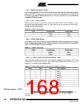
SPI Data Register – SPDR
Bit
7
SPD7
R/W
X
6
SPD6
R/W
X
5
SPD5
R/W
X
4
SPD4
R/W
X
3
SPD3
R/W
X
2
SPD2
R/W
X
1
SPD1
R/W
X
0
SPD0
R/W
X
SPDR
Read/Write
Initial Value
Undefined
• Bits 7:0 - SPD7:0: SPI Data
The SPI Data Register is a read/write register used for data transfer between the Regis-
ter File and the SPI Shift Register. Writing to the register initiates data transmission.
Reading the register causes the Shift Register Receive buffer to be read.
169
4250E–CAN–12/04

 ATMEL [ ATMEL ]