AT90CAN128
recovery units are used for asynchronous data reception. In addition to the recovery
units, the Receiver includes a Parity Checker, Control logic, a Shift Register and a two
level receive buffer (UDRn). The Receiver supports the same frame formats as the
Transmitter, and can detect Frame Error, Data OverRun and Parity Errors.
Clock Generation
The Clock Generation logic generates the base clock for the Transmitter and Receiver.
The USARTn supports four modes of clock operation: Normal asynchronous, Double
Speed asynchronous, Master synchronous and Slave synchronous mode. The UMSELn
bit in USARTn Control and Status Register C (UCSRnC) selects between asynchronous
and synchronous operation. Double Speed (asynchronous mode only) is controlled by
the U2Xn found in the UCSRnA Register. When using synchronous mode (UMSELn =
1), the Data Direction Register for the XCKn pin (DDR_XCKn) controls whether the
clock source is internal (Master mode) or external (Slave mode). The XCKn pin is only
active when using synchronous mode.
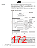
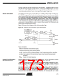
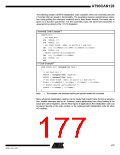
Figure 84 shows a block diagram of the clock generation logic.
Figure 84. USARTn Clock Generation Logic, Block Diagram
UBRRn
U2Xn
fclkio
UBRRn+1
Prescaling
Down-Counter
/2
/4
/2
0
1
0
1
clkio
txn clk
UMSELn
rxn clk
DDR_XCKn
Sync
Register
Edge
Detector
0
1
xn cki
XCKn
Pin
xn cko
DDR_XCKn
UCPOLn
1
0
Signal description:
txn clk Transmitter clock (Internal Signal).
rxn clk Receiver base clock (Internal Signal).
xn cki Input from XCK pin (internal Signal). Used for synchronous slave operation.
xn cko Clock output to XCK pin (Internal Signal). Used for synchronous master
operation.
fclkio System I/O Clock frequency.
Internal Clock Generation –
Baud Rate Generator
Internal clock generation is used for the asynchronous and the synchronous master
modes of operation. The description in this section refers to Figure 84.
The USARTn Baud Rate Register (UBRRn) and the down-counter connected to it func-
tion as a programmable prescaler or baud rate generator. The down-counter, running at
system clock (fclkio), is loaded with the UBRRn value each time the counter has counted
down to zero or when the UBRRnL Register is written. A clock is generated each time
the counter reaches zero. This clock is the baud rate generator clock output (=
fclkio/(UBRRn+1)). The Transmitter divides the baud rate generator clock output by 2, 8
or 16 depending on mode. The baud rate generator output is used directly by the
Receiver’s clock and data recovery units. However, the recovery units use a state
173
4250E–CAN–12/04

 ATMEL [ ATMEL ]