B10011S
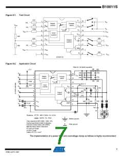
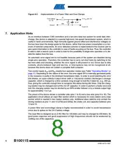
All the logical and sensing functions in the device are powered by VDD = 5V. Therefore, the filter
section also acts as a level shifter to the input comparator range (approximately 1 to 3.3V). The
diagram (see Figure 7-1) shows how the battery voltage, VCC, influences the comparator input
voltages, F0 and F1, in relation to the internal reference voltage, Vref, in the recessive state.
The lower VCC, the lower the bus level. Taking this into account the comparator input levels are
F1 – Vref for single-wire H respectively F1 – F0 for two-wire operation. The comparator’s offset
voltage is ≤10 mV. Matching the filter biasing to the internal reference is essentially for safe
operation even at low battery voltages during motor start.
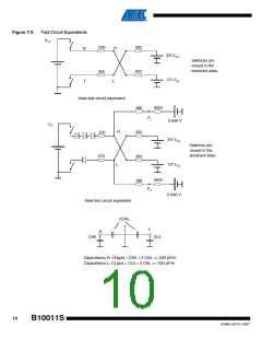
The level investigations and tests described in the following description have been carried out
within the temperature range of –40°C to +105°C with two B10011S on a bus line, one of them
always in the recessive state (see Figure 7-2 on page 10).
In case of line shorts to VCC or to ground or in case of H to L shorts, all participants on the bus
are intended to switch to single-wire operation and to disable their drivers not in use.
The dynamic behavior of the circuit depends on the line capacitances to ground. Approximately
200 pF/m and a maximum of 6 nF have to be taken into account. The transition from the domi-
nant to the recessive state enables the bias network to recharge the line through a driving
resistor of approximately 300Ω. The transition from the recessive to the dominant state is
approximately twice as fast. This is probably the source of emitted radiation having no capaci-
tance on the line. The choke coil enables the suppression of this radiation in the frequency range
above 5 MHz to 7 MHz. Care should be taken not to feed noise from VDD or VCC to the line.
Therefore, they should be properly blocked by low-inductance capacitors.
Data loss by externally induced interference is avoided by careful PCB layout and EMC design
for this circuit as well as by providing appropriate overvoltage protection. It is very essential to
separate battery ground and filter ground as indicated in the application circuit (see Figure 6-2
on page 7). Especially important is that the filter ground must be connected to pin 8 by a short
connection not subject to disturbing currents from external sources. The ground wire of the “star-
quad” cable may introduce such currents and should be connected to battery ground via a
0.1-µF capacitor in a way as short as possible, perhaps to the metal housing.
In order to avoid thermal problems, the voltage divider and driving resistors should be kept away
from the IC. Otherwise they would heat up the environment of the small IC and might reduce its
life expectancy.
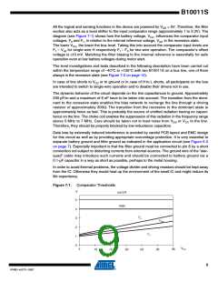
Figure 7-1. Comparator Thresholds
V
not ER
RxN
5
4
3
2
1
0
F0
Uref
F1
VCC
5
35
10
15
20
25
30
9
4749D–AUTO–10/07

 ATMEL [ ATMEL ]