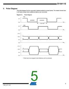
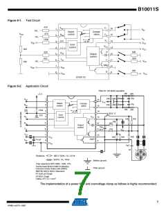
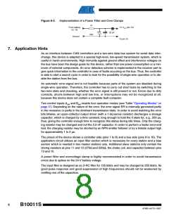
Figure 6-3. Implementation of a Power Filter and Over Clamps
10
From battery
(cl. 15)
To VCC (pin 13)
+
22 µF
33V
Ground
To pin 10
7. Application Hints
As an interface between CAN controllers and a two-wire data bus system for serial data inter-
change, this device is adapted to a special high-level, low-speed transmission system, which is
useful in harsh environments. High immunity against ground offset and interference voltages on
the bus have been the design goals for this device, rather than low power consumption or a min-
imum of external components. An error detection scheme is implemented in the receiver part to
give quick information to the controller in case of faults occurring on the bus. Thus, the controller
is able to start a search cycle in order to look for the possibility of single-wire operation or to dis-
able the station from the bus.
An automatic error-signal end is not feasible because parts of the system are disabled during
single-wire operation. Therefore, the controller has to carry out short tests by switching to the
two-wire state and checking, whether the error signal is still present or not. Errors due to dirty
contacts, shorts between high and low line, or interruptions may not be recognized at all,
because this device does not contain a complete fault computer.
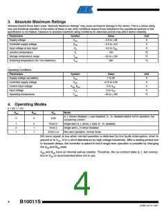
Two control inputs Asel and Bsel enable four operation modes (see Table “Operating Modes” on
page 4’). Depending on the nature of the error, the error signal ER is internally generated partly
in the recessive or partly in the dominant transmission state. In order to avoid watching the error
bits bitwise, an open-collector output driver (with a 1-kΩ series resistor) discharges a storage
capacitor, which is charged by a time constant, long enough to hold the 0 state for, e.g., 200 µs,
thus, giving the controller enough time to recognize this status during idle times. Only the charg-
ing resistor may be changed and not the 2.2-nF capacitor. In order to perform a faster error-end
test, the charging resistor may be shorted by an NPN emitter follower or by a tristate output high
for approximately 1 to 2 µs.
The pinout of the device shows a controller side (pins 1 to 8) and a bus side (pins 9 to 16). The
application circuit utilizes an input filter section which is necessary for every station and a bias
section which is needed in two master stations only. Additional slave stations only contain the
driving resistors at pins 11 and 12 (270Ω and 220Ω), the choke coil, and capacitor between pins
13 and 10.
A power filter and overvoltage clamp is highly recommended in order to avoid transmission
errors due to spikes on the 24-V battery voltage.
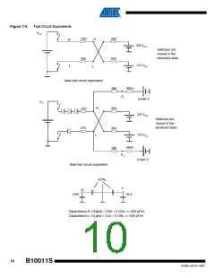
The input filter is designed as an 2-RC filter for 125 kbit/s and may be changed to 250 kbit/s. Its
good pulse response and good suppression of high frequencies should not be weakened by
omitting one of the capacitors.
8
B10011S
4749D–AUTO–10/07

 ATMEL [ ATMEL ]