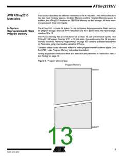
SRAM Data Memory
Figure 9 shows how the ATtiny2313 SRAM Memory is organized.
The lower 224 data memory locations address both the Register File, the I/O memory,
Extended I/O memory, and the internal data SRAM. The first 32 locations address the
Register File, the next 64 location the standard I/O memory, and the next 128 locations
address the internal data SRAM.
The five different addressing modes for the data memory cover: Direct, Indirect with Dis-
placement, Indirect, Indirect with Pre-decrement, and Indirect with Post-increment. In
the Register File, registers R26 to R31 feature the indirect addressing pointer registers.
The direct addressing reaches the entire data space.
The Indirect with Displacement mode reaches 63 address locations from the base
address given by the Y- or Z-register.
When using register indirect addressing modes with automatic pre-decrement and post-
increment, the address registers X, Y, and Z are decremented or incremented.
The 32 general purpose working registers, 64 I/O Registers, and the 128 bytes of inter-
nal data SRAM in the ATtiny2313 are all accessible through all these addressing
modes. The Register File is described in “General Purpose Register File” on page 8.
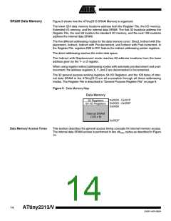
Figure 9. Data Memory Map
Data Memory
0x0000 - 0x001F
0x0020 - 0x005F
0x0060
32 Registers
64 I/O Registers
Internal SRAM
(128 x 8)
0x00DF
Data Memory Access Times
This section describes the general access timing concepts for internal memory access.
The internal data SRAM access is performed in two clkCPU cycles as described in Figure
10.
14
ATtiny2313/V
2543F–AVR–08/04

 ATMEL [ ATMEL ]