Stack Pointer
The Stack is mainly used for storing temporary data, for storing local variables and for
storing return addresses after interrupts and subroutine calls. The Stack Pointer Regis-
ter always points to the top of the Stack. Note that the Stack is implemented as growing
from higher memory locations to lower memory locations. This implies that a Stack
PUSH command decreases the Stack Pointer.
The Stack Pointer points to the data SRAM Stack area where the Subroutine and Inter-
rupt Stacks are located. This Stack space in the data SRAM must be defined by the
program before any subroutine calls are executed or interrupts are enabled. The Stack
Pointer must be set to point above 0x60. The Stack Pointer is decremented by one
when data is pushed onto the Stack with the PUSH instruction, and it is decremented by
two when the return address is pushed onto the Stack with subroutine call or interrupt.
The Stack Pointer is incremented by one when data is popped from the Stack with the
POP instruction, and it is incremented by two when data is popped from the Stack with
return from subroutine RET or return from interrupt RETI.
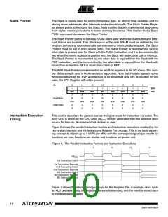
The AVR Stack Pointer is implemented as two 8-bit registers in the I/O space. The num-
ber of bits actually used is implementation dependent. Note that the data space in some
implementations of the AVR architecture is so small that only SPL is needed. In this
case, the SPH Register will not be present.
Bit
15
–
14
–
13
–
12
–
11
–
10
–
9
–
8
–
SPH
SPL
SP7
7
SP6
6
SP5
5
SP4
4
SP3
3
SP2
2
SP1
1
SP0
0
Read/Write
Initial Value
R
R
R
R
R
R
R
R
R/W
0
R/W
0
R/W
0
R/W
0
R/W
0
R/W
0
R/W
0
R/W
0
0
0
0
0
0
0
0
0
Instruction Execution
Timing
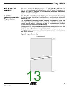
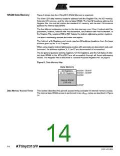
This section describes the general access timing concepts for instruction execution. The
AVR CPU is driven by the CPU clock clkCPU, directly generated from the selected clock
source for the chip. No internal clock division is used.
Figure 6 shows the parallel instruction fetches and instruction executions enabled by the
Harvard architecture and the fast-access Register File concept. This is the basic pipelin-
ing concept to obtain up to 1 MIPS per MHz with the corresponding unique results for
functions per cost, functions per clocks, and functions per power-unit.
Figure 6. The Parallel Instruction Fetches and Instruction Executions
T1
T2
T3
T4
clkCPU
1st Instruction Fetch
1st Instruction Execute
2nd Instruction Fetch
2nd Instruction Execute
3rd Instruction Fetch
3rd Instruction Execute
4th Instruction Fetch
Figure 7 shows the internal timing concept for the Register File. In a single clock cycle
an ALU operation using two register operands is executed, and the result is stored back
to the destination register.
10
ATtiny2313/V
2543F–AVR–08/04

 ATMEL [ ATMEL ]