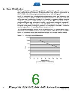
ATmega16M1/32M1/32C1/64M1/64C1 Automotive
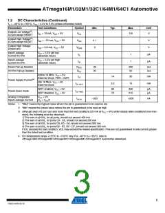
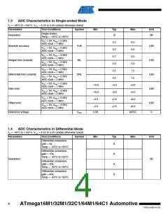
1.2
DC Characteristics (Continued)
TA = –40°C to +150°C, VCC = 4.5V to 5.5V (unless otherwise noted)
Parameters
Test Conditions
Symbol
Min.
Typ.
Max.
Unit
Output Low Voltage(3),
I/O pin except RESET
IOL = 10 mA, VCC = 5V
VOL
0.8
V
Output High Voltage(4),
I/O pin except RESET
I
OH = –10 mA, VCC = 5V
VOH
VOH3
IIL
4.1
3
V
V
Output High Voltage
(Reset pin)
IOH = 0.6 mA, VCC = 5V
Input Leakage
Current I/O Pin
VCC = 5.5V, pin low
(absolute value)
1
1
µA
µA
Input Leakage
Current I/O Pin
VCC = 5.5V, pin high
(absolute value)
IIH
Reset Pull-up Resistor
I/O Pin Pull-up Resistor
RRST
RPU
30
20
200
50
kΩ
kΩ
Active 16 MHz, VCC = 5V,
External Clock, PRR = 0xFF,
ICC
14
30
15
mA
mA
Power Supply Current(4)
Power-down mode
Idle 16 MHz, VCC = 5V,
External Clock
ICC IDLE
5.5
WDT enabled, VCC = 5V
WDT disabled, VCC = 5V
80
70
330
310
µA
µA
ICC PWD
IACLK
Analog Comparator
Input Leakage Current
VCC = 5V
Vin = VCC/2
–200
+200
nA
Notes: 1. “Max” means the highest value where the pin is guaranteed to be read as low
2. “Min” means the lowest value where the pin is guaranteed to be read as high
3. Although each I/O port can sink more than the test conditions (20 mA at VCC = 5V) under steady state conditions (non-tran-
sient), the following must be observed:
1] The sum of all IOL, for all ports, should not exceed 400 mA.
2] The sum of all IOL, for ports C0 - C5, should not exceed 200 mA.
3] The sum of all IOL, for ports C6, D0 - D4, should not exceed 300 mA.
4] The sum of all IOL, for ports B0 - B7, D5 - D7, should not exceed 300 mA.
If IOL exceeds the test condition, VOL may exceed the related specification. Pins are not guaranteed to sink current greater
than the listed test condition.
4. For temperature range +125°C to +150°C only. For –40°C to +125°C, refer to
ATmega16M1/ATmega32M1/ATmega32C1/ATmega64M1/ATmega64C1 Automotive datasheet.
3
7781D–AVR–01/10

 ATMEL [ ATMEL ]