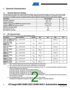
1. Electrical Characteristics
1.1
Absolute Maximum Ratings
Stresses beyond those listed under “Absolute Maximum Ratings” may cause permanent damage to the device. This is a stress rating
only and functional operation of the device at these or any other conditions beyond those indicated in the operational sections of this
specification is not implied. Exposure to absolute maximum rating conditions for extended periods may affect device reliability.
Parameters
Test Conditions
–55 to +150
–65 to +175
–0.5 to VCC+0.5
–0.5 to +13.0
6.0
Unit
°C
°C
V
Operating Temperature
Storage Temperature
Voltage on any Pin except RESET with respect to Ground
Voltage on RESET with respect to Ground
Maximum Operating Voltage
V
V
DC Current per I/O Pin
DC Current VCC and GND
30
200.0
mA
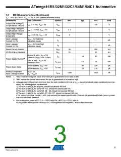
1.2
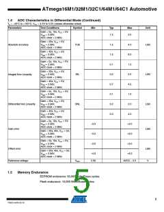
DC Characteristics
TA = –40°C to +150°C, VCC = 4.5V to 5.5V (unless otherwise noted)
Parameters
Test Conditions
Symbol
Min.
Typ.
Max.
Unit
Input Low Voltage, except
XTAL1 and RESET pin
(1)
VCC = 4.5V to 5.5V
VIL
–0.5
+0.2VCC
V
Input High Voltage,
except XTAL1 and
RESET pins
(2)
V
CC = 4.5V to 5.5V
CC = 4.5V to 5.5V
VIH
0.6VCC
VCC + 0.5
V
Input Low Voltage,
XTAL1 pin
(1)
V
VIL1
VIH1
VIL2
VIH2
VIL3
VIH3
–0.5
0.8VCC
–0.5
+0.1VCC
V
V
V
V
V
V
Input High Voltage,
XTAL1 pin
(2)
(2)
(2)
VCC = 4.5V to 5.5V
VCC = 4.5V to 5.5V
VCC + 0.5
Input Low Voltage,
RESET pin
(1)
+0.2VCC
Input High Voltage,
RESET pin
VCC = 4.5V to 5.5V
0.9VCC
–0.5
VCC + 0.5
Input Low Voltage,
RESET pin as I/O
(1)
VCC = 4.5V to 5.5V
VCC = 4.5V to 5.5V
+0.2VCC
Input High Voltage,
RESET pin as I/O
0.8VCC
VCC + 0.5
Notes: 1. “Max” means the highest value where the pin is guaranteed to be read as low
2. “Min” means the lowest value where the pin is guaranteed to be read as high
3. Although each I/O port can sink more than the test conditions (20 mA at VCC = 5V) under steady state conditions (non-tran-
sient), the following must be observed:
1] The sum of all IOL, for all ports, should not exceed 400 mA.
2] The sum of all IOL, for ports C0 - C5, should not exceed 200 mA.
3] The sum of all IOL, for ports C6, D0 - D4, should not exceed 300 mA.
4] The sum of all IOL, for ports B0 - B7, D5 - D7, should not exceed 300 mA.
If IOL exceeds the test condition, VOL may exceed the related specification. Pins are not guaranteed to sink current greater
than the listed test condition.
4. For temperature range +125°C to +150°C only. For –40°C to +125°C, refer to
ATmega16M1/ATmega32M1/ATmega32C1/ATmega64M1/ATmega64C1 Automotive datasheet.
2
ATmega16M1/32M1/32C1/64M1/64C1 Automotive
7781D–AVR–01/10

 ATMEL [ ATMEL ]