ATmega64A
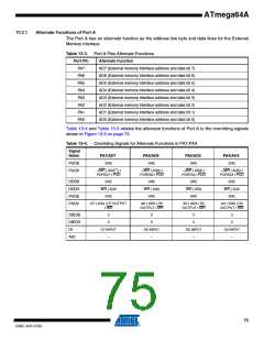
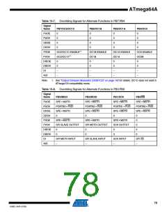
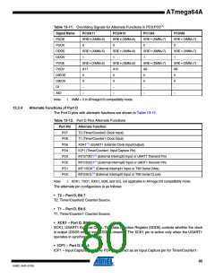
Table 13-5. Overriding Signals for Alternate Functions in PA3:PA0(1)
Signal
Name
PUOE
PUOV
PA3/AD3
PA2/AD2
PA1/AD1
PA0/AD0
SRE
SRE
SRE
SRE
~(WR | ADA) •
PORTA3 • PUD
~(WR | ADA) •
PORTA2 • PUD
~(WR | ADA) •
PORTA1 • PUD
~(WR | ADA) •
PORTA0 • PUD
SRE
WR | ADA
SRE
SRE
WR | ADA
SRE
SRE
WR | ADA
SRE
SRE
WR | ADA
SRE
DDOE
DDOV
PVOE
PVOV
A3 • ADA | D3
OUTPUT • WR
A2• ADA | D2
OUTPUT • WR
A1 • ADA | D1
OUTPUT • WR
A0 • ADA | D0
OUTPUT • WR
0
0
0
0
DIEOE
DIEOV
DI
0
D3 INPUT
–
0
D2 INPUT
–
0
D1 INPUT
–
0
D0 INPUT
–
AIO
Note:
1. ADA is short for ADdress Active and represents the time when address is output. See “Exter-
nal Memory Interface” on page 23 for details.
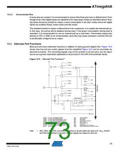
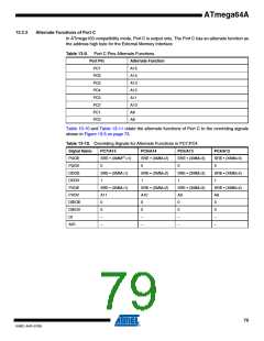
13.3.2
Alternate Functions of Port B
The Port B pins with alternate functions are shown in Table 13-6.
Table 13-6. Port B Pins Alternate Functions
Port Pin
Alternate Functions
PB7
OC2/OC1C(1) (Output Compare and PWM Output for Timer/Counter2 or Output Compare
and PWM Output C for Timer/Counter1)
PB6
PB5
PB4
PB3
PB2
PB1
PB0
OC1B (Output Compare and PWM Output B for Timer/Counter1)
OC1A (Output Compare and PWM Output A for Timer/Counter1)
OC0 (Output Compare and PWM Output for Timer/Counter0)
MISO (SPI Bus Master Input/Slave Output)
MOSI (SPI Bus Master Output/Slave Input)
SCK (SPI Bus Serial Clock)
SS (SPI Slave Select input)
Note:
1. OC1C not applicable in ATmega103 compatibility mode.
The alternate pin configuration is as follows:
• OC2/OC1C, Bit 7
OC2, Output Compare Match output: The PB7 pin can serve as an external output for the
Timer/Counter2 Output Compare. The pin has to be configured as an output (DDB7 set (one)) to
serve this function. The OC2 pin is also the output pin for the PWM mode timer function.
OC1C, Output Compare Match C output: The PB7 pin can serve as an external output for the
Timer/Counter1 Output Compare C. The pin has to be configured as an output (DDB7 set (one))
to serve this function. The OC1C pin is also the output pin for the PWM mode timer function.
76
8160C–AVR–07/09

 ATMEL [ ATMEL ]