ATmega64A
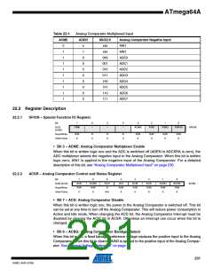
Table 22-1. Analog Comparator Multiplexed Input
ACME
ADEN
MUX2:0
xxx
Analog Comparator Negative Input
0
1
1
1
1
1
1
1
1
1
x
1
0
0
0
0
0
0
0
0
AIN1
xxx
AIN1
000
001
010
011
100
101
110
111
ADC0
ADC1
ADC2
ADC3
ADC4
ADC5
ADC6
ADC7
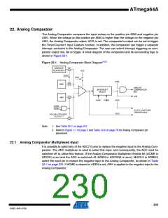
22.2 Register Description
22.2.1
SFIOR – Special Function IO Register
Bit
7
6
5
4
3
2
1
0
0x20
TSM
–
–
–
ACME
PUD
PSR2
PSR10
SFIOR
(0x40)
Read/Write
Initial Value
R/W
0
R
0
R
0
R
0
R/W
0
R/W
0
R/W
0
R/W
0
• Bit 3 – ACME: Analog Comparator Multiplexer Enable
When this bit is written logic one and the ADC is switched off (ADEN in ADCSRA is zero), the
ADC multiplexer selects the negative input to the Analog Comparator. When this bit is written
logic zero, AIN1 is applied to the negative input of the Analog Comparator. For a detailed
description of this bit, see “Analog Comparator Multiplexed Input” on page 230.
22.2.2
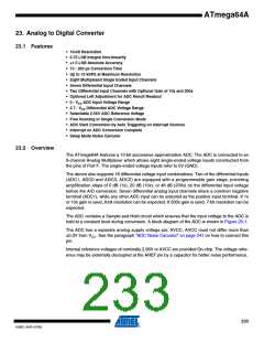
ACSR – Analog Comparator Control and Status Register
Bit
0x08 (0x28)
7
6
5
4
3
ACIE
R/W
0
2
ACIC
R/W
0
1
ACIS1
R/W
0
0
ACIS0
R/W
0
ACD
ACBG
ACO
ACI
R/W
0
ACSR
Read/Write
Initial Value
R/W
0
R/W
0
R
N/A
• Bit 7 – ACD: Analog Comparator Disable
When this bit is written logic one, the power to the Analog Comparator is switched off. This bit
can be set at any time to turn off the Analog Comparator. This will reduce power consumption in
Active and Idle mode. When changing the ACD bit, the Analog Comparator Interrupt must be
disabled by clearing the ACIE bit in ACSR. Otherwise an interrupt can occur when the bit is
changed.
• Bit 6 – ACBG: Analog Comparator Bandgap Select
When this bit is set, a fixed bandgap reference voltage replaces the positive input to the Analog
Comparator. When this bit is cleared, AIN0 is applied to the positive input of the Analog Compar-
ator. See “Internal Voltage Reference” on page 55.
231
8160C–AVR–07/09

 ATMEL [ ATMEL ]