ATmega64A
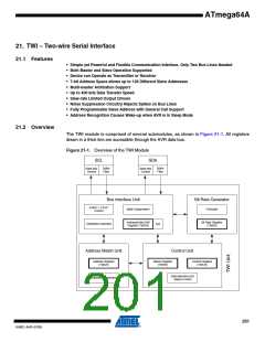
21.2.1
21.2.2
SCL and SDA Pins
These pins interface the AVR TWI with the rest of the MCU system. The output drivers contain a
slew-rate limiter in order to conform to the TWI specification. The input stages contain a spike
suppression unit removing spikes shorter than 50 ns. Note that the internal pull-ups in the AVR
pads can be enabled by setting the PORT bits corresponding to the SCL and SDA pins, as
explained in the I/O Port section. The internal pull-ups can in some systems eliminate the need
for external ones.
Bit Rate Generator Unit
This unit controls the period of SCL when operating in a Master mode. The SCL period is con-
trolled by settings in the TWI Bit Rate Register (TWBR) and the Prescaler bits in the TWI Status
Register (TWSR). Slave operation does not depend on Bit Rate or Prescaler settings, but the
CPU clock frequency in the slave must be at least 16 times higher than the SCL frequency. Note
that slaves may prolong the SCL low period, thereby reducing the average TWI bus clock
period. The SCL frequency is generated according to the following equation:
CPU Clock frequency
SCL frequency = -----------------------------------------------------------
TWPS
16 + 2(TWBR) ⋅ 4
• TWBR = Value of the TWI Bit Rate Register.
• TWPS = Value of the prescaler bits in the TWI Status Register.
Note:
Pull-up resistor values should be selected according to the SCL frequency and the capacitive bus
line load. See Table 28-4 on page 331 for value of pull-up resistor."
21.2.3
Bus Interface Unit
This unit contains the Data and Address Shift Register (TWDR), a START/STOP Controller and
Arbitration detection hardware. The TWDR contains the address or data bytes to be transmitted,
or the address or data bytes received. In addition to the 8-bit TWDR, the Bus Interface Unit also
contains a register containing the (N)ACK bit to be transmitted or received. This (N)ACK Regis-
ter is not directly accessible by the application software. However, when receiving, it can be set
or cleared by manipulating the TWI Control Register (TWCR). When in Transmitter mode, the
value of the received (N)ACK bit can be determined by the value in the TWSR.
The START/STOP Controller is responsible for generation and detection of START, REPEATED
START, and STOP conditions. The START/STOP controller is able to detect START and STOP
conditions even when the AVR MCU is in one of the sleep modes, enabling the MCU to wake up
if addressed by a Master.
If the TWI has initiated a transmission as Master, the Arbitration Detection hardware continu-
ously monitors the transmission trying to determine if arbitration is in process. If the TWI has lost
an arbitration, the Control Unit is informed. Correct action can then be taken and appropriate
status codes generated.
21.2.4
Address Match Unit
The Address Match unit checks if received address bytes match the 7-bit address in the TWI
Address Register (TWAR). If the TWI General Call Recognition Enable (TWGCE) bit in the
TWAR is written to one, all incoming address bits will also be compared against the General Call
address. Upon an address match, the Control unit is informed, allowing correct action to be
taken. The TWI may or may not acknowledge its address, depending on settings in the TWCR.
202
8160C–AVR–07/09

 ATMEL [ ATMEL ]