ATmega48PA/88PA/168PA/328P
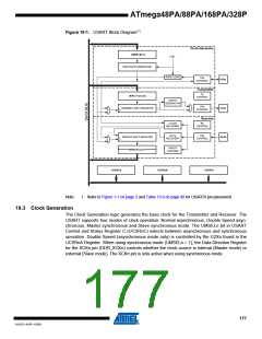
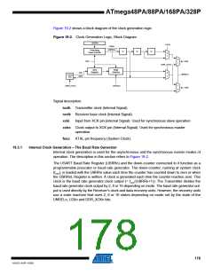
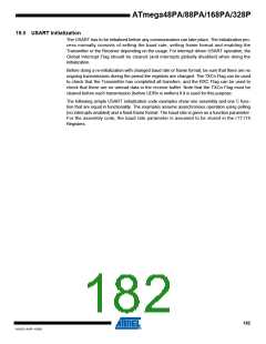
Figure 19-2 shows a block diagram of the clock generation logic.
Figure 19-2. Clock Generation Logic, Block Diagram
UBRRn
U2Xn
foscn
UBRRn+1
Prescaling
Down-Counter
/2
/4
/2
0
1
0
1
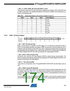
OSC
txclk
UMSELn
rxclk
DDR_XCKn
Sync
Register
Edge
Detector
xcki
0
1
XCKn
Pin
xcko
DDR_XCKn
UCPOLn
1
0
Signal description:
txclk Transmitter clock (Internal Signal).
rxclk Receiver base clock (Internal Signal).
xcki
Input from XCK pin (internal Signal). Used for synchronous slave operation.
xcko Clock output to XCK pin (Internal Signal). Used for synchronous master
operation.
fosc
XTAL pin frequency (System Clock).
19.3.1
Internal Clock Generation – The Baud Rate Generator
Internal clock generation is used for the asynchronous and the synchronous master modes of
operation. The description in this section refers to Figure 19-2.
The USART Baud Rate Register (UBRRn) and the down-counter connected to it function as a
programmable prescaler or baud rate generator. The down-counter, running at system clock
(fosc), is loaded with the UBRRn value each time the counter has counted down to zero or when
the UBRRnL Register is written. A clock is generated each time the counter reaches zero. This
clock is the baud rate generator clock output (= fosc/(UBRRn+1)). The Transmitter divides the
baud rate generator clock output by 2, 8 or 16 depending on mode. The baud rate generator out-
put is used directly by the Receiver’s clock and data recovery units. However, the recovery units
use a state machine that uses 2, 8 or 16 states depending on mode set by the state of the
UMSELn, U2Xn and DDR_XCKn bits.
178
8161D–AVR–10/09

 ATMEL [ ATMEL ]