ATmega48PA/88PA/168PA/328P
19. USART0
19.1 Features
• Full Duplex Operation (Independent Serial Receive and Transmit Registers)
• Asynchronous or Synchronous Operation
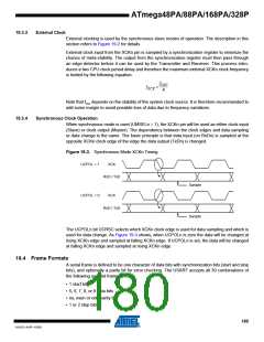
• Master or Slave Clocked Synchronous Operation
• High Resolution Baud Rate Generator
• Supports Serial Frames with 5, 6, 7, 8, or 9 Data Bits and 1 or 2 Stop Bits
• Odd or Even Parity Generation and Parity Check Supported by Hardware
• Data OverRun Detection
• Framing Error Detection
• Noise Filtering Includes False Start Bit Detection and Digital Low Pass Filter
• Three Separate Interrupts on TX Complete, TX Data Register Empty and RX Complete
• Multi-processor Communication Mode
• Double Speed Asynchronous Communication Mode
19.2 Overview
The Universal Synchronous and Asynchronous serial Receiver and Transmitter (USART) is a
highly flexible serial communication device.
The USART0 can also be used in Master SPI mode, see “USART in SPI Mode” on page 204.
The Power Reduction USART bit, PRUSART0, in ”Minimizing Power Consumption” on page 42
must be disabled by writing a logical zero to it.
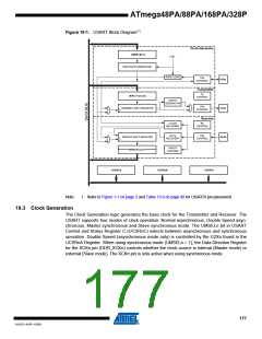
A simplified block diagram of the USART Transmitter is shown in Figure 19-1 on page 177. CPU
accessible I/O Registers and I/O pins are shown in bold.
The dashed boxes in the block diagram separate the three main parts of the USART (listed from
the top): Clock Generator, Transmitter and Receiver. Control Registers are shared by all units.
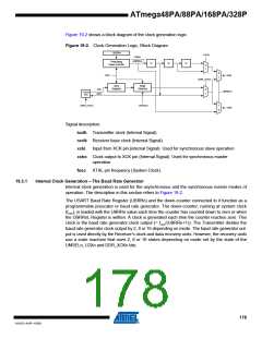
The Clock Generation logic consists of synchronization logic for external clock input used by
synchronous slave operation, and the baud rate generator. The XCKn (Transfer Clock) pin is
only used by synchronous transfer mode. The Transmitter consists of a single write buffer, a
serial Shift Register, Parity Generator and Control logic for handling different serial frame for-
mats. The write buffer allows a continuous transfer of data without any delay between frames.
The Receiver is the most complex part of the USART module due to its clock and data recovery
units. The recovery units are used for asynchronous data reception. In addition to the recovery
units, the Receiver includes a Parity Checker, Control logic, a Shift Register and a two level
receive buffer (UDRn). The Receiver supports the same frame formats as the Transmitter, and
can detect Frame Error, Data OverRun and Parity Errors.
176
8161D–AVR–10/09

 ATMEL [ ATMEL ]