ATmega8(L)
Timer/Counter 1 –
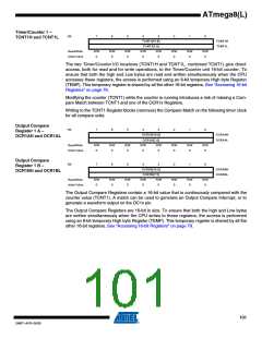
TCNT1H and TCNT1L
Bit
7
6
5
4
3
2
1
0
TCNT1[15:8]
TCNT1[7:0]
TCNT1H
TCNT1L
R/W
Read/Write
Initial Value
R/W
0
R/W
0
R/W
0
R/W
R/W
R/W
0
R/W
0
0
0
0
The two Timer/Counter I/O locations (TCNT1H and TCNT1L, combined TCNT1) give direct
access, both for read and for write operations, to the Timer/Counter unit 16-bit counter. To
ensure that both the high and Low bytes are read and written simultaneously when the CPU
accesses these registers, the access is performed using an 8-bit temporary High byte Register
(TEMP). This temporary register is shared by all the other 16-bit registers. See “Accessing 16-bit
Registers” on page 79.
Modifying the counter (TCNT1) while the counter is running introduces a risk of missing a Com-
pare Match between TCNT1 and one of the OCR1x Registers.
Writing to the TCNT1 Register blocks (removes) the Compare Match on the following timer clock
for all compare units.
Output Compare
Register 1 A –
OCR1AH and OCR1AL
Bit
7
6
5
4
3
2
1
0
OCR1A[15:8]
OCR1A[7:0]
OCR1AH
OCR1AL
Read/Write
Initial Value
R/W
0
R/W
0
R/W
0
R/W
R/W
0
R/W
0
R/W
0
R/W
0
0
Output Compare
Register 1 B –
OCR1BH and OCR1BL
Bit
7
6
5
4
3
2
1
0
OCR1B[15:8]
OCR1B[7:0]
OCR1BH
OCR1BL
Read/Write
Initial Value
R/W
0
R/W
0
R/W
0
R/W
R/W
0
R/W
0
R/W
0
R/W
0
0
The Output Compare Registers contain a 16-bit value that is continuously compared with the
counter value (TCNT1). A match can be used to generate an Output Compare Interrupt, or to
generate a waveform output on the OC1x pin.
The Output Compare Registers are 16-bit in size. To ensure that both the high and Low bytes
are written simultaneously when the CPU writes to these registers, the access is performed
using an 8-bit temporary High byte Register (TEMP). This temporary register is shared by all the
other 16-bit registers. See “Accessing 16-bit Registers” on page 79.
101
2486T–AVR–05/08

 ATMEL [ ATMEL ]