Using the ICR1 Register for defining TOP works well when using fixed TOP values. By using
ICR1, the OCR1A Register is free to be used for generating a PWM output on OC1A. However,
if the base PWM frequency is actively changed by changing the TOP value, using the OCR1A as
TOP is clearly a better choice due to its double buffer feature.
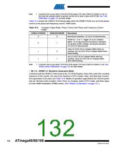
In phase and frequency correct PWM mode, the compare units allow generation of PWM wave-
forms on the OC1x pins. Setting the COM1x1:0 bits to two will produce a non-inverted PWM and
an inverted PWM output can be generated by setting the COM1x1:0 to three (See Table on
page 132). The actual OC1x value will only be visible on the port pin if the data direction for the
port pin is set as output (DDR_OC1x). The PWM waveform is generated by setting (or clearing)
the OC1x Register at the compare match between OCR1x and TCNT1 when the counter incre-
ments, and clearing (or setting) the OC1x Register at compare match between OCR1x and
TCNT1 when the counter decrements. The PWM frequency for the output when using phase
and frequency correct PWM can be calculated by the following equation:
f
clk_I/O
f
= ---------------------------
OCnxPFCPWM
2 ⋅ N ⋅ TOP
The N variable represents the prescaler divider (1, 8, 64, 256, or 1024).
The extreme values for the OCR1x Register represents special cases when generating a PWM
waveform output in the phase correct PWM mode. If the OCR1x is set equal to BOTTOM the
output will be continuously low and if set equal to TOP the output will be set to high for non-
inverted PWM mode. For inverted PWM the output will have the opposite logic values. If OCR1A
is used to define the TOP value (WGM13:0 = 9) and COM1A1:0 = 1, the OC1A output will toggle
with a 50% duty cycle.
15.10 Timer/Counter Timing Diagrams
The Timer/Counter is a synchronous design and the timer clock (clkT1) is therefore shown as a
clock enable signal in the following figures. The figures include information on when Interrupt
Flags are set, and when the OCR1x Register is updated with the OCR1x buffer value (only for
modes utilizing double buffering). Figure 15-10 shows a timing diagram for the setting of OCF1x.
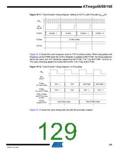
Figure 15-10. Timer/Counter Timing Diagram, Setting of OCF1x, no Prescaling
clkI/O
clkTn
(clkI/O/1)
TCNTn
OCRnx
OCFnx
OCRnx - 1
OCRnx
OCRnx + 1
OCRnx + 2
OCRnx Value
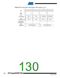
Figure 15-11 shows the same timing data, but with the prescaler enabled.
128
ATmega48/88/168
2545M–AVR–09/07

 ATMEL [ ATMEL ]