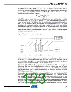
ATmega48/88/168
the maximum resolution is 16-bit (ICR1 or OCR1A set to MAX). The PWM resolution in bits can
be calculated using the following equation:
log(TOP + 1)
R
= ----------------------------------
PFCPWM
log(2)
In phase and frequency correct PWM mode the counter is incremented until the counter value
matches either the value in ICR1 (WGM13:0 = 8), or the value in OCR1A (WGM13:0 = 9). The
counter has then reached the TOP and changes the count direction. The TCNT1 value will be
equal to TOP for one timer clock cycle. The timing diagram for the phase correct and frequency
correct PWM mode is shown on Figure 15-9. The figure shows phase and frequency correct
PWM mode when OCR1A or ICR1 is used to define TOP. The TCNT1 value is in the timing dia-
gram shown as a histogram for illustrating the dual-slope operation. The diagram includes non-
inverted and inverted PWM outputs. The small horizontal line marks on the TCNT1 slopes repre-
sent compare matches between OCR1x and TCNT1. The OC1x Interrupt Flag will be set when a
compare match occurs.
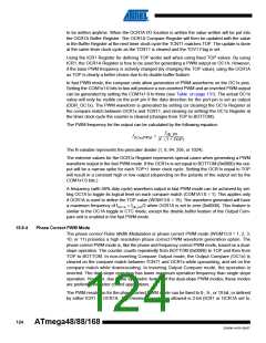
Figure 15-9. Phase and Frequency Correct PWM Mode, Timing Diagram
OCnA Interrupt Flag Set
or ICFn Interrupt Flag Set
(Interrupt on TOP)
OCRnx/TOP Updateand
TOVn Interrupt Flag Set
(Interrupt on Bottom)
TCNTn
(COMnx1:0 = 2)
OCnx
(COMnx1:0 = 3)
OCnx
1
2
3
4
Period
The Timer/Counter Overflow Flag (TOV1) is set at the same timer clock cycle as the OCR1x
Registers are updated with the double buffer value (at BOTTOM). When either OCR1A or ICR1
is used for defining the TOP value, the OC1A or ICF1 Flag set when TCNT1 has reached TOP.
The Interrupt Flags can then be used to generate an interrupt each time the counter reaches the
TOP or BOTTOM value.
When changing the TOP value the program must ensure that the new TOP value is higher or
equal to the value of all of the Compare Registers. If the TOP value is lower than any of the
Compare Registers, a compare match will never occur between the TCNT1 and the OCR1x.
As Figure 15-9 shows the output generated is, in contrast to the phase correct mode, symmetri-
cal in all periods. Since the OCR1x Registers are updated at BOTTOM, the length of the rising
and the falling slopes will always be equal. This gives symmetrical output pulses and is therefore
frequency correct.
127
2545M–AVR–09/07

 ATMEL [ ATMEL ]