ATmega8(L)
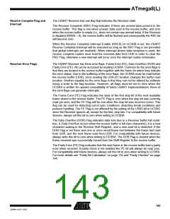
(U2X = 1) of operation. Samples denoted zero are samples done when the RxD line is
idle (i.e., no communication activity).
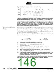
Figure 65. Start Bit Sampling
RxD
IDLE
START
BIT 0
Sample
(U2X = 0)
0
0
1
1
2
3
2
4
5
3
6
7
4
8
9
5
10
11
6
12
13
7
14
15
8
16
1
1
2
3
Sample
(U2X = 1)
0
2
When the clock recovery logic detects a high (idle) to low (start) transition on the RxD
line, the start bit detection sequence is initiated. Let sample 1 denote the first zero-
sample as shown in the figure. The clock recovery logic then uses samples 8, 9 and 10
for Normal mode, and samples 4, 5 and 6 for Double Speed mode (indicated with
sample numbers inside boxes on the figure), to decide if a valid start bit is received. If
two or more of these three samples have logical high levels (the majority wins), the start
bit is rejected as a noise spike and the Receiver starts looking for the next high to low-
transition. If however, a valid start bit is detected, the clock recovery logic is
synchronized and the data recovery can begin. The synchronization process is repeated
for each start bit.
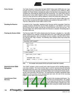
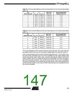
Asynchronous Data Recovery When the Receiver clock is synchronized to the start bit, the data recovery can begin.
The data recovery unit uses a state machine that has 16 states for each bit in Normal
mode and eight states for each bit in Double Speed mode. Figure 66 shows the sam-
pling of the data bits and the parity bit. Each of the samples is given a number that is
equal to the state of the recovery unit.
Figure 66. Sampling of Data and Parity Bit
RxD
BIT n
Sample
(U2X = 0)
1
1
2
3
2
4
5
3
6
7
4
8
9
5
10
11
6
12
13
7
14
15
8
16
1
1
Sample
(U2X = 1)
The decision of the logic level of the received bit is taken by doing a majority voting of
the logic value to the three samples in the center of the received bit. The center samples
are emphasized on the figure by having the sample number inside boxes. The majority
voting process is done as follows: If two or all three samples have high levels, the
received bit is registered to be a logic 1. If two or all three samples have low levels, the
received bit is registered to be a logic 0. This majority voting process acts as a low pass
filter for the incoming signal on the RxD pin. The recovery process is then repeated until
a complete frame is received. Including the first stop bit. Note that the Receiver only
uses the first stop bit of a frame.
Figure 67 shows the sampling of the stop bit and the earliest possible beginning of the
start bit of the next frame.
145
2486M–AVR–12/03

 ATMEL [ ATMEL ]