Parity Checker
The Parity Checker is active when the high USART Parity mode (UPM1) bit is set. Type
of parity check to be performed (odd or even) is selected by the UPM0 bit. When
enabled, the Parity Checker calculates the parity of the data bits in incoming frames and
compares the result with the parity bit from the serial frame. The result of the check is
stored in the receive buffer together with the received data and stop bits. The Parity
Error (PE) Flag can then be read by software to check if the frame had a parity error.
The PE bit is set if the next character that can be read from the receive buffer had a par-
ity error when received and the parity checking was enabled at that point (UPM1 = 1).
This bit is valid until the receive buffer (UDR) is read.
Disabling the Receiver
In contrast to the Transmitter, disabling of the Receiver will be immediate. Data from
ongoing receptions will therefore be lost. When disabled (i.e., the RXEN is set to zero)
the Receiver will no longer override the normal function of the RxD port pin. The
Receiver buffer FIFO will be flushed when the Receiver is disabled. Remaining data in
the buffer will be lost
Flushing the Receive Buffer
The Receiver buffer FIFO will be flushed when the Receiver is disabled (i.e., the buffer
will be emptied of its contents). Unread data will be lost. If the buffer has to be flushed
during normal operation, due to for instance an error condition, read the UDR I/O loca-
tion until the RXC Flag is cleared. The following code example shows how to flush the
receive buffer.
Assembly Code Example(1)
USART_Flush:
sbis UCSRA, RXC
ret
in
rjmp USART_Flush
C Code Example(1)
r16, UDR
void USART_Flush( void )
{
unsigned char dummy;
while ( UCSRA & (1<<RXC) ) dummy = UDR;
}
Note:
1. The example code assumes that the part specific header file is included.
Asynchronous Data
Reception
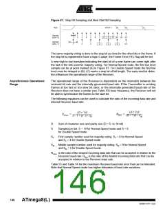
The USART includes a clock recovery and a data recovery unit for handling asynchro-
nous data reception. The clock recovery logic is used for synchronizing the internally
generated baud rate clock to the incoming asynchronous serial frames at the RxD pin.
The data recovery logic samples and low pass filters each incoming bit, thereby improv-
ing the noise immunity of the Receiver. The asynchronous reception operational range
depends on the accuracy of the internal baud rate clock, the rate of the incoming
frames, and the frame size in number of bits.
Asynchronous Clock
Recovery
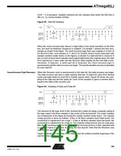
The clock recovery logic synchronizes internal clock to the incoming serial frames. Fig-
ure 65 illustrates the sampling process of the start bit of an incoming frame. The sample
rate is 16 times the baud rate for Normal mode, and eight times the baud rate for Double
Speed mode. The horizontal arrows illustrate the synchronization variation due to the
sampling process. Note the larger time variation when using the Double Speed mode
144
ATmega8(L)
2486M–AVR–12/03

 ATMEL [ ATMEL ]