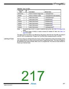
ATmega8(L)
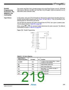
Parallel
Programming
Enter Programming
Mode
The following algorithm puts the device in Parallel Programming mode:
1. Apply 4.5V - 5.5V between VCC and GND, and wait at least 100µs
2. Set RESET to “0” and toggle XTAL1 at least 6 times
3. Set the Prog_enable pins listed in Table 92 on page 220 to “0000” and wait at least
100ns
4. Apply 11.5V - 12.5V to RESET. Any activity on Prog_enable pins within 100ns after +12V
has been applied to RESET, will cause the device to fail entering Programming mode
Note, if the RESET pin is disabled by programming the RSTDISBL Fuse, it may not be possible
to follow the proposed algorithm above. The same may apply when External Crystal or External
RC configuration is selected because it is not possible to apply qualified XTAL1 pulses. In such
cases, the following algorithm should be followed:
1. Set Prog_enable pins listed in Table 92 on page 220 to “0000”
2. Apply 4.5V - 5.5V between VCC and GND simultaneously as 11.5V - 12.5V is applied to
RESET
3. Wait 100ns
4. Re-program the fuses to ensure that External Clock is selected as clock source
(CKSEL3:0 = 0’b0000) and RESET pin is activated (RSTDISBL unprogrammed). If Lock
Bits are programmed, a chip erase command must be executed before changing the
fuses
5. Exit Programming mode by power the device down or by bringing RESET pin to 0’b0
6. Entering Programming mode with the original algorithm, as described above
Considerations for
The loaded command and address are retained in the device during programming. For efficient
Efficient Programming programming, the following should be considered.
•
•
•
The command needs only be loaded once when writing or reading multiple memory
locations
Skip writing the data value 0xFF, that is the contents of the entire EEPROM (unless the
EESAVE Fuse is programmed) and Flash after a Chip Erase
Address High byte needs only be loaded before programming or reading a new 256 word
window in Flash or 256 byte EEPROM. This consideration also applies to Signature bytes
reading
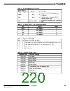
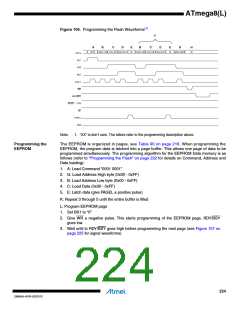
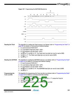
Chip Erase
The Chip Erase will erase the Flash and EEPROM(1) memories plus Lock Bits. The Lock Bits are
not reset until the Program memory has been completely erased. The Fuse Bits are not
changed. A Chip Erase must be performed before the Flash and/or the EEPROM are
reprogrammed.
Note:
1. The EEPRPOM memory is preserved during chip erase if the EESAVE Fuse is programmed
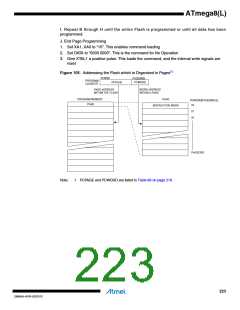
Load Command “Chip Erase”
1. Set XA1, XA0 to “10”. This enables command loading
2. Set BS1 to “0”
3. Set DATA to “1000 0000”. This is the command for Chip Erase
4. Give XTAL1 a positive pulse. This loads the command
5. Give WR a negative pulse. This starts the Chip Erase. RDY/BSY goes low
6. Wait until RDY/BSY goes high before loading a new command
221
2486AA–AVR–02/2013

 ATMEL [ ATMEL ]