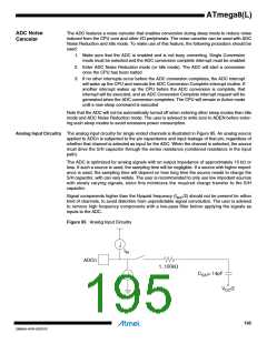
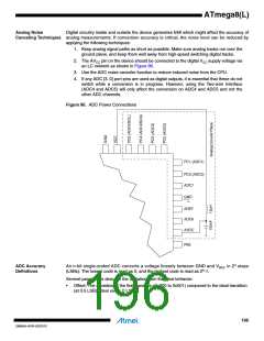
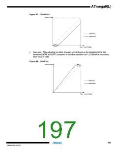
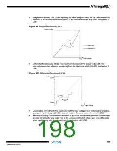
ATmega8(L)
ADC Conversion
Result
After the conversion is complete (ADIF is high), the conversion result can be found in the ADC
Result Registers (ADCL, ADCH).
For single ended conversion, the result is:
V
1024
IN
ADC = --------------------------
V
REF
where VIN is the voltage on the selected input pin and VREF the selected voltage reference (see
Table 74 and Table 75). 0x000 represents ground, and 0x3FF represents the selected reference
voltage minus one LSB.
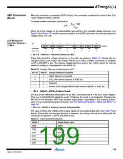
ADC Multiplexer
Selection Register –
ADMUX
Bit
7
REFS1
R/W
0
6
REFS0
R/W
0
5
ADLAR
R/W
0
4
–
3
MUX3
R/W
0
2
MUX2
R/W
0
1
MUX1
R/W
0
0
MUX0
R/W
0
ADMUX
Read/Write
Initial Value
R
0
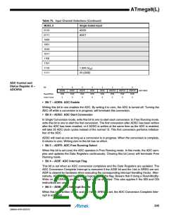
• Bit 7:6 – REFS1:0: Reference Selection Bits
These bits select the voltage reference for the ADC, as shown in Table 74. If these bits are
changed during a conversion, the change will not go in effect until this conversion is complete
(ADIF in ADCSRA is set). The internal voltage reference options may not be used if an external
reference voltage is being applied to the AREF pin.
Table 74. Voltage Reference Selections for ADC
REFS1
REFS0 Voltage Reference Selection
0
0
1
1
0
1
0
1
AREF, Internal Vref turned off
AVCC with external capacitor at AREF pin
Reserved
Internal 2.56V Voltage Reference with external capacitor at AREF pin
•
Bit 5 – ADLAR: ADC Left Adjust Result
The ADLAR bit affects the presentation of the ADC conversion result in the ADC Data Register.
Write one to ADLAR to left adjust the result. Otherwise, the result is right adjusted. Changing the
ADLAR bit will affect the ADC Data Register immediately, regardless of any ongoing conver-
sions. For a complete description of this bit, see “The ADC Data Register – ADCL and ADCH” on
page 201.
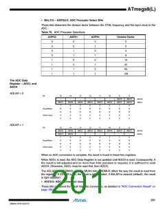
• Bits 3:0 – MUX3:0: Analog Channel Selection Bits
The value of these bits selects which analog inputs are connected to the ADC. See Table 75 for
details. If these bits are changed during a conversion, the change will not go in effect until this
conversion is complete (ADIF in ADCSRA is set).
Table 75. Input Channel Selections
MUX3..0
0000
Single Ended Input
ADC0
0001
ADC1
0010
ADC2
0011
ADC3
0100
ADC4
0101
ADC5
199
2486AA–AVR–02/2013

 ATMEL [ ATMEL ]