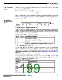
ATmega8(L)
ADC Noise
Canceler
The ADC features a noise canceler that enables conversion during sleep mode to reduce noise
induced from the CPU core and other I/O peripherals. The noise canceler can be used with ADC
Noise Reduction and Idle mode. To make use of this feature, the following procedure should be
used:
1. Make sure that the ADC is enabled and is not busy converting. Single Conversion
mode must be selected and the ADC conversion complete interrupt must be enabled
2. Enter ADC Noise Reduction mode (or Idle mode). The ADC will start a conversion
once the CPU has been halted
3. If no other interrupts occur before the ADC conversion completes, the ADC interrupt
will wake up the CPU and execute the ADC Conversion Complete interrupt routine. If
another interrupt wakes up the CPU before the ADC conversion is complete, that
interrupt will be executed, and an ADC Conversion Complete interrupt request will be
generated when the ADC conversion completes. The CPU will remain in Active mode
until a new sleep command is executed
Note that the ADC will not be automatically turned off when entering other sleep modes than Idle
mode and ADC Noise Reduction mode. The user is advised to write zero to ADEN before enter-
ing such sleep modes to avoid excessive power consumption.
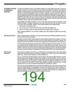
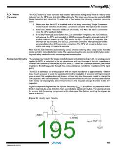
Analog Input Circuitry The analog input circuitry for single ended channels is illustrated in Figure 95. An analog source
applied to ADCn is subjected to the pin capacitance and input leakage of that pin, regardless of
whether that channel is selected as input for the ADC. When the channel is selected, the source
must drive the S/H capacitor through the series resistance (combined resistance in the input
path).
The ADC is optimized for analog signals with an output impedance of approximately 10 k or
less. If such a source is used, the sampling time will be negligible. If a source with higher imped-
ance is used, the sampling time will depend on how long time the source needs to charge the
S/H capacitor, with can vary widely. The user is recommended to only use low impedant sources
with slowly varying signals, since this minimizes the required charge transfer to the S/H
capacitor.
Signal components higher than the Nyquist frequency (fADC/2) should not be present for either
kind of channels, to avoid distortion from unpredictable signal convolution. The user is advised
to remove high frequency components with a low-pass filter before applying the signals as
inputs to the ADC.
Figure 95. Analog Input Circuitry
I
IH
ADCn
1..100kΩ
C
= 14pF
S/H
I
IL
V
/2
CC
195
2486AA–AVR–02/2013

 ATMEL [ ATMEL ]