ATmega48/88/168
Note that enabling the alternate function of some of the port pins does not affect the use
of the other pins in the port as general digital I/O.
Ports as General Digital
I/O
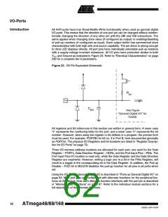
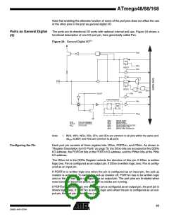
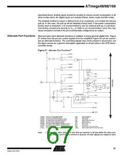
The ports are bi-directional I/O ports with optional internal pull-ups. Figure 24 shows a
functional description of one I/O-port pin, here generically called Pxn.
Figure 24. General Digital I/O(1)
PUD
Q
D
DDxn
Q CLR
WDx
RDx
RESET
1
0
Q
D
Pxn
PORTxn
Q CLR
RESET
WPx
WRx
SLEEP
RRx
SYNCHRONIZER
RPx
D
Q
D
L
Q
Q
PINxn
Q
clk I/O
WDx:
RDx:
WRx:
RRx:
RPx:
WPx:
WRITE DDRx
READ DDRx
WRITE PORTx
PUD:
PULLUP DISABLE
SLEEP CONTROL
I/O CLOCK
SLEEP:
clkI/O
:
READ PORTx REGISTER
READ PORTx PIN
WRITE PINx REGISTER
Note:
1. WRx, WPx, WDx, RRx, RPx, and RDx are common to all pins within the same port.
clkI/O, SLEEP, and PUD are common to all ports.
Configuring the Pin
Each port pin consists of three register bits: DDxn, PORTxn, and PINxn. As shown in
“Register Description for I/O Ports” on page 79, the DDxn bits are accessed at the DDRx
I/O address, the PORTxn bits at the PORTx I/O address, and the PINxn bits at the PINx
I/O address.
The DDxn bit in the DDRx Register selects the direction of this pin. If DDxn is written
logic one, Pxn is configured as an output pin. If DDxn is written logic zero, Pxn is config-
ured as an input pin.
If PORTxn is written logic one when the pin is configured as an input pin, the pull-up
resistor is activated. To switch the pull-up resistor off, PORTxn has to be written logic
zero or the pin has to be configured as an output pin. The port pins are tri-stated when
reset condition becomes active, even if no clocks are running.
If PORTxn is written logic one when the pin is configured as an output pin, the port pin is
driven high (one). If PORTxn is written logic zero when the pin is configured as an out-
put pin, the port pin is driven low (zero).
63
2545D–AVR–07/04

 ATMEL [ ATMEL ]