tions. This is also the case if the Reset Vector is in the Application section while the
Interrupt Vectors are in the Boot section or vice versa.
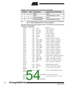
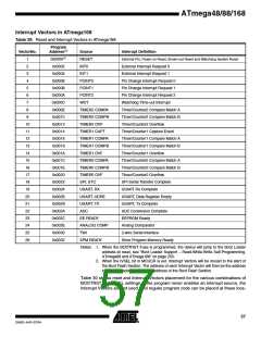
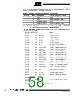
Table 30. Reset and Interrupt Vectors Placement in ATmega168(1)
BOOTRST
IVSEL
Reset Address
0x000
Interrupt Vectors Start Address
0x001
1
1
0
0
0
1
0
1
0x000
Boot Reset Address + 0x0002
0x001
Boot Reset Address
Boot Reset Address
Boot Reset Address + 0x0002
Note:
1. The Boot Reset Address is shown in Table 109 on page 268. For the BOOTRST
Fuse “1” means unprogrammed while “0” means programmed.
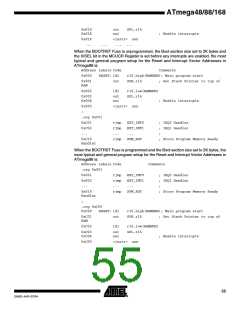
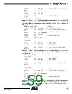
The most typical and general program setup for the Reset and Interrupt Vector
Addresses in ATmega168 is:
Address Labels Code
Comments
0x0000
0x0002
0x0004
0x0006
0x0008
0x000A
0x000C
0x000E
0x0010
0x0012
0x0014
0x0016
0x0018
0x001A
0x001C
0x001E
0x0020
0x0022
0x0024
0x0026
0x0028
jmp
jmp
jmp
jmp
jmp
jmp
jmp
jmp
jmp
jmp
jmp
jmp
jmp
jmp
jmp
jmp
jmp
jmp
jmp
jmp
jmp
jmp
RESET
; Reset Handler
EXT_INT0
EXT_INT1
PCINT0
; IRQ0 Handler
; IRQ1 Handler
; PCINT0 Handler
PCINT1
; PCINT1 Handler
PCINT2
; PCINT2 Handler
WDT
; Watchdog Timer Handler
; Timer2 Compare A Handler
; Timer2 Compare B Handler
; Timer2 Overflow Handler
; Timer1 Capture Handler
; Timer1 Compare A Handler
; Timer1 Compare B Handler
; Timer1 Overflow Handler
; Timer0 Compare A Handler
; Timer0 Compare B Handler
; Timer0 Overflow Handler
; SPI Transfer Complete Handler
; USART, RX Complete Handler
; USART, UDR Empty Handler
; USART, TX Complete Handler
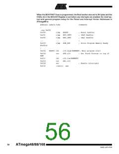
; ADC Conversion Complete
TIM2_COMPA
TIM2_COMPB
TIM2_OVF
TIM1_CAPT
TIM1_COMPA
TIM1_COMPB
TIM1_OVF
TIM0_COMPA
TIM0_COMPB
TIM0_OVF
SPI_STC
USART_RXC
USART_UDRE
USART_TXC
ADC
0x002A
Handler
0x002C
0x002E
jmp
jmp
jmp
EE_RDY
ANA_COMP
TWI
; EEPROM Ready Handler
; Analog Comparator Handler
; 2-wire Serial Interface
0x0030
Handler
0x0032
Handler
jmp
ldi
SPM_RDY
; Store Program Memory Ready
;
0x0033RESET:
r16, high(RAMEND); Main program start
58
ATmega48/88/168
2545D–AVR–07/04

 ATMEL [ ATMEL ]