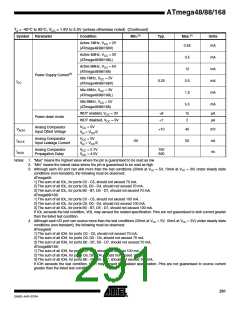
ATmega48/88/168
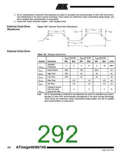
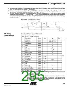
5. This requirement applies to all ATmega48/88/168 2-wire Serial Interface operation. Other devices connected to the 2-wire
Serial Bus need only obey the general fSCL requirement.
6. The actual low period generated by the ATmega48/88/168 2-wire Serial Interface is (1/fSCL - 2/fCK), thus fCK must be greater
than 6 MHz for the low time requirement to be strictly met at fSCL = 100 kHz.
7. The actual low period generated by the ATmega48/88/168 2-wire Serial Interface is (1/fSCL - 2/fCK), thus the low time require-
ment will not be strictly met for fSCL > 308 kHz when fCK = 8 MHz. Still, ATmega48/88/168 devices connected to the bus may
communicate at full speed (400 kHz) with other ATmega48/88/168 devices, as well as any other device with a proper tLOW
acceptance margin.
Figure 133. 2-wire Serial Bus Timing
t
HIGH
t
t
r
of
t
t
LOW
LOW
SCL
SDA
t
t
t
HD;DAT
SU;STA
HD;STA
t
SU;DAT
t
SU;STO
t
BUF
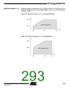
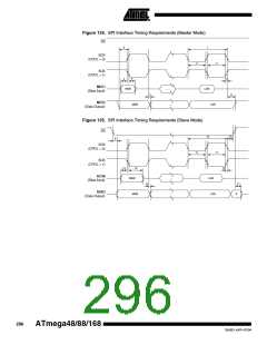
SPI Timing
See Figure 134 and Figure 135 for details.
Characteristics
Table 134. SPI Timing Parameters
Description
SCK period
SCK high/low
Rise/Fall time
Setup
Mode
Master
Master
Master
Master
Master
Master
Master
Master
Slave
Min
Typ
Max
1
2
See Table 71
50ꢀ duty cycle
3
3.6
10
4
5
Hold
10
6
Out to SCK
SCK to out
SCK to out high
SS low to out
SCK period
SCK high/low(1)
Rise/Fall time
Setup
0.5 • tsck
10
7
8
10
9
15
ns
10
11
12
13
14
15
16
17
Slave
4 • tck
2 • tck
Slave
Slave
1600
Slave
10
tck
Hold
Slave
SCK to out
SCK to SS high
SS high to tri-state
SS low to SCK
Slave
15
10
Slave
20
Slave
18
Slave
20
Note:
1. In SPI Programming mode the minimum SCK high/low period is:
- 2 tCLCL for fCK < 12 MHz
- 3 tCLCL for fCK > 12 MHz
2. All DC Characteristics contained in this datasheet are based on simulation and char-
acterization of other AVR microcontrollers manufactured in the same process
technology. These values are preliminary values representing design targets, and will
be updated after characterization of actual silicon.
295
2545D–AVR–07/04

 ATMEL [ ATMEL ]