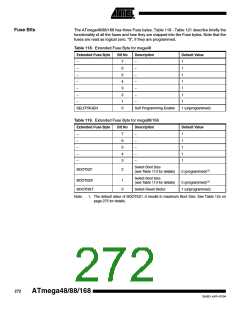
ATmega48/88/168
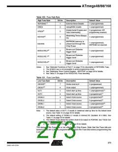
Table 120. Fuse High Byte
High Fuse Byte
RSTDISBL(1)
DWEN
Bit No
Description
Default Value
7
6
External Reset Disable
debugWIRE Enable
1 (unprogrammed)
1 (unprogrammed)
Enable Serial Program and
Data Downloading
0 (programmed, SPI
programming enabled)
SPIEN(2)
5
4
Watchdog Timer Always
On
WDTON(3)
1 (unprogrammed)
EEPROM memory is
preserved through the
Chip Erase
1 (unprogrammed),
EEPROM not reserved
EESAVE
3
Brown-out Detector
trigger level
BODLEVEL2(4)
BODLEVEL1(4)
BODLEVEL0(4)
2
1
0
1 (unprogrammed)
1 (unprogrammed)
1 (unprogrammed)
Brown-out Detector
trigger level
Brown-out Detector
trigger level
Notes: 1. See “Alternate Functions of Port C” on page 73 for description of RSTDISBL Fuse.
2. The SPIEN Fuse is not accessible in serial programming mode.
3. See “Watchdog Timer Control Register - WDTCSR” on page 49 for details.
4. See Table 21 on page 43 for BODLEVEL Fuse decoding.
Table 121. Fuse Low Byte
Low Fuse Byte
CKDIV8(4)
CKOUT(3)
SUT1
Bit No
Description
Default Value
7
6
5
4
3
2
1
0
Divide clock by 8
Clock output
0 (programmed)
1 (unprogrammed)
1 (unprogrammed)(1)
0 (programmed)(1)
0 (programmed)(2)
0 (programmed)(2)
1 (unprogrammed)(2)
0 (programmed)(2)
Select start-up time
Select start-up time
Select Clock source
Select Clock source
Select Clock source
Select Clock source
SUT0
CKSEL3
CKSEL2
CKSEL1
CKSEL0
Note:
1. The default value of SUT1..0 results in maximum start-up time for the default clock
source. See Table 12 on page 30 for details.
2. The default setting of CKSEL3..0 results in internal RC Oscillator @ 8 MHz. See
Table 11 on page 30 for details.
3. The CKOUT Fuse allows the system clock to be output on PORTB0. See “Clock Out-
put Buffer” on page 32 for details.
4. See “System Clock Prescaler” on page 33 for details.
The status of the Fuse bits is not affected by Chip Erase. Note that the Fuse bits are
locked if Lock bit1 (LB1) is programmed. Program the Fuse bits before programming the
Lock bits.
273
2545D–AVR–07/04

 ATMEL [ ATMEL ]