ATmega48/88/168
USART in SPI Mode
The Universal Synchronous and Asynchronous serial Receiver and Transmitter
(USART) can be set to a master SPI compliant mode of operation. The Master SPI
Mode (MSPIM) has the following features:
• Full Duplex, Three-wire Synchronous Data Transfer
• Master Operation
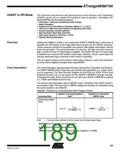
• Supports all four SPI Modes of Operation (Mode 0, 1, 2, and 3)
• LSB First or MSB First Data Transfer (Configurable Data Order)
• Queued Operation (Double Buffered)
• High Resolution Baud Rate Generator
• High Speed Operation (fXCKmax = fCK/2)
• Flexible Interrupt Generation
Overview
Setting both UMSELn1:0 bits to one enables the USART in MSPIM logic. In this mode of
operation the SPI master control logic takes direct control over the USART resources.
These resources include the transmitter and receiver shift register and buffers, and the
baud rate generator. The parity generator and checker, the data and clock recovery
logic, and the RX and TX control logic is disabled. The USART RX and TX control logic
is replaced by a common SPI transfer control logic. However, the pin control logic and
interrupt generation logic is identical in both modes of operation.
The I/O register locations are the same in both modes. However, some of the functional-
ity of the control registers changes when using MSPIM.
Clock Generation
The Clock Generation logic generates the base clock for the Transmitter and Receiver.
For USART MSPIM mode of operation only internal clock generation (i.e. master opera-
tion) is supported. The Data Direction Register for the XCKn pin (DDR_XCKn) must
therefore be set to one (i.e. as output) for the USART in MSPIM to operate correctly.
Preferably the DDR_XCKn should be set up before the USART in MSPIM is enabled
(i.e. TXENn and RXENn bit set to one).
The internal clock generation used in MSPIM mode is identical to the USART synchro-
nous master mode. The baud rate or UBRRn setting can therefore be calculated using
the same equations, see Table 85:
Table 85. Equations for Calculating Baud Rate Register Setting
Equation for Calculating Baud
Rate(1)
Equation for Calculating
UBRRn Value
Operating Mode
Synchronous Master
mode
f
OSC
f
OSC
BAUD = --------------------------------------
UBRRn = -------------------- – 1
2(UBRRn + 1)
2BAUD
Note:
BAUD Baud rate (in bits per second, bps)
fOSC System Oscillator clock frequency
UBRRnContents of the UBRRnH and UBRRnL Registers, (0-4095)
1. The baud rate is defined to be the transfer rate in bit per second (bps)
189
2545D–AVR–07/04

 ATMEL [ ATMEL ]