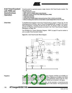
When the ICR1 is used as TOP value (see description of the WGM13:0 bits located in
the TCCR1A and the TCCR1B Register), the ICP1 is disconnected and consequently
the Input Capture function is disabled.
• Bit 5 – Reserved Bit
This bit is reserved for future use. For ensuring compatibility with future devices, this bit
must be written to zero when TCCR1B is written.
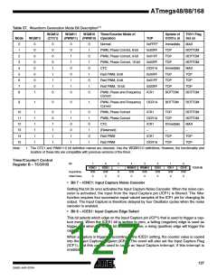
• Bit 4:3 – WGM13:2: Waveform Generation Mode
See TCCR1A Register description.
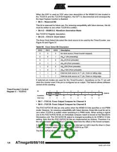
• Bit 2:0 – CS12:0: Clock Select
The three Clock Select bits select the clock source to be used by the Timer/Counter, see
Figure 50 and Figure 51.
Table 58. Clock Select Bit Description
CS12
CS11
CS10
Description
0
0
0
0
1
1
1
1
0
0
1
1
0
0
1
1
0
1
0
1
0
1
0
1
No clock source (Timer/Counter stopped).
clkI/O/1 (No prescaling)
clkI/O/8 (From prescaler)
clkI/O/64 (From prescaler)
clkI/O/256 (From prescaler)
clkI/O/1024 (From prescaler)
External clock source on T1 pin. Clock on falling edge.
External clock source on T1 pin. Clock on rising edge.
If external pin modes are used for the Timer/Counter1, transitions on the T1 pin will
clock the counter even if the pin is configured as an output. This feature allows software
control of the counting.
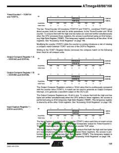
Timer/Counter1 Control
Register C – TCCR1C
Bit
7
FOC1A
R/W
0
6
FOC1B
R/W
0
5
–
4
–
3
–
2
–
1
–
0
–
TCCR1C
Read/Write
Initial Value
R
0
R
0
R
0
R
0
R
0
R
0
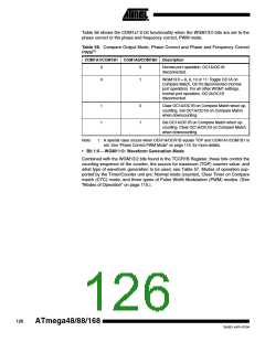
• Bit 7 – FOC1A: Force Output Compare for Channel A
• Bit 6 – FOC1B: Force Output Compare for Channel B
The FOC1A/FOC1B bits are only active when the WGM13:0 bits specifies a non-PWM
mode. However, for ensuring compatibility with future devices, these bits must be set to
zero when TCCR1A is written when operating in a PWM mode. When writing a logical
one to the FOC1A/FOC1B bit, an immediate compare match is forced on the Waveform
Generation unit. The OC1A/OC1B output is changed according to its COM1x1:0 bits
setting. Note that the FOC1A/FOC1B bits are implemented as strobes. Therefore it is
the value present in the COM1x1:0 bits that determine the effect of the forced compare.
A FOC1A/FOC1B strobe will not generate any interrupt nor will it clear the timer in Clear
Timer on Compare match (CTC) mode using OCR1A as TOP.
The FOC1A/FOC1B bits are always read as zero.
128
ATmega48/88/168
2545D–AVR–07/04

 ATMEL [ ATMEL ]