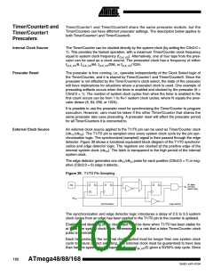
also set the Compare Match Flag (OCF1A/B) which can be used to generate an Output
Compare interrupt request.
The Input Capture Register can capture the Timer/Counter value at a given external
(edge triggered) event on either the Input Capture pin (ICP1) or on the Analog Compar-
ator pins (See “Analog Comparator” on page 228.) The Input Capture unit includes a
digital filtering unit (Noise Canceler) for reducing the chance of capturing noise spikes.
The TOP value, or maximum Timer/Counter value, can in some modes of operation be
defined by either the OCR1A Register, the ICR1 Register, or by a set of fixed values.
When using OCR1A as TOP value in a PWM mode, the OCR1A Register can not be
used for generating a PWM output. However, the TOP value will in this case be double
buffered allowing the TOP value to be changed in run time. If a fixed TOP value is
required, the ICR1 Register can be used as an alternative, freeing the OCR1A to be
used as PWM output.
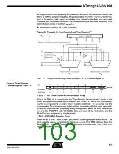
Definitions
The following definitions are used extensively throughout the section:
Table 53. Definitions
BOTTOM The counter reaches the BOTTOM when it becomes 0x0000.
MAX
TOP
The counter reaches its MAXimum when it becomes 0xFFFF (decimal 65535).
The counter reaches the TOP when it becomes equal to the highest value in the
count sequence. The TOP value can be assigned to be one of the fixed values:
0x00FF, 0x01FF, or 0x03FF, or to the value stored in the OCR1A or ICR1 Regis-
ter. The assignment is dependent of the mode of operation.
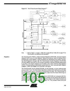
Accessing 16-bit
Registers
The TCNT1, OCR1A/B, and ICR1 are 16-bit registers that can be accessed by the AVR
CPU via the 8-bit data bus. The 16-bit register must be byte accessed using two read or
write operations. Each 16-bit timer has a single 8-bit register for temporary storing of the
high byte of the 16-bit access. The same temporary register is shared between all 16-bit
registers within each 16-bit timer. Accessing the low byte triggers the 16-bit read or write
operation. When the low byte of a 16-bit register is written by the CPU, the high byte
stored in the temporary register, and the low byte written are both copied into the 16-bit
register in the same clock cycle. When the low byte of a 16-bit register is read by the
CPU, the high byte of the 16-bit register is copied into the temporary register in the
same clock cycle as the low byte is read.
Not all 16-bit accesses uses the temporary register for the high byte. Reading the
OCR1A/B 16-bit registers does not involve using the temporary register.
To do a 16-bit write, the high byte must be written before the low byte. For a 16-bit read,
the low byte must be read before the high byte.
The following code examples show how to access the 16-bit Timer Registers assuming
that no interrupts updates the temporary register. The same principle can be used
directly for accessing the OCR1A/B and ICR1 Registers. Note that when using “C”, the
compiler handles the 16-bit access.
106
ATmega48/88/168
2545D–AVR–07/04

 ATMEL [ ATMEL ]