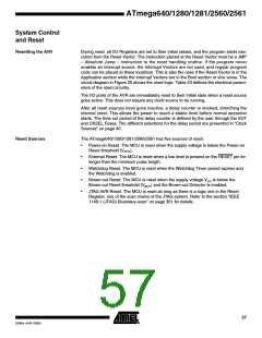
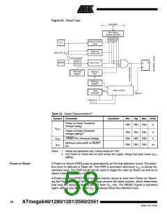
Figure 25. Reset Logic
DATA BUS
MCU Status
Register (MCUSR)
Power-on Reset
Circuit
Brown-out
Reset Circuit
BODLEVEL [2..0]
Pull-up Resistor
SPIKE
FILTER
JTAG Reset
Register
Watchdog
Oscillator
Delay Counters
Clock
CK
Generator
TIMEOUT
CKSEL[3:0]
SUT[1:0]
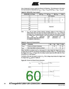
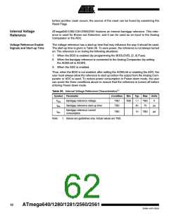
Table 23. Reset Characteristics(1)
Symbol Parameter
Condition
Min
Typ
Max Units
Power-on Reset Threshold
Voltage (rising)
TBD TBD TBD
V
VPOT
Power-on Reset Threshold
TBD TBD TBD
TBD TBD TBD
TBD TBD TBD
V
V
Voltage (falling)(2)
VRST
tRST
RESET Pin Threshold Voltage
Minimum pulse width on RESET
Pin
ns
Notes: 1. Values are guidelines only. Actual values are TBD.
2. The Power-on Reset will not work unless the supply voltage has been below VPOT
(falling)
Power-on Reset
A Power-on Reset (POR) pulse is generated by an On-chip detection circuit. The detec-
tion level is defined in Table 23. The POR is activated whenever VCC is below the
detection level. The POR circuit can be used to trigger the start-up Reset, as well as to
detect a failure in supply voltage.
A Power-on Reset (POR) circuit ensures that the device is reset from Power-on. Reach-
ing the Power-on Reset threshold voltage invokes the delay counter, which determines
how long the device is kept in RESET after VCC rise. The RESET signal is activated
again, without any delay, when VCC decreases below the detection level.
58
ATmega640/1280/1281/2560/2561
2549A–AVR–03/05

 ATMEL [ ATMEL ]