ATmega640/1280/1281/2560/2561
PROG_COMMANDS (0x5)
The AVR specific public JTAG instruction for entering programming commands via the
JTAG port. The 15-bit Programming Command Register is selected as Data Register.
The active states are the following:
•
•
Capture-DR: The result of the previous command is loaded into the Data Register.
Shift-DR: The Data Register is shifted by the TCK input, shifting out the result of the
previous command and shifting in the new command.
•
•
Update-DR: The programming command is applied to the Flash inputs
Run-Test/Idle: One clock cycle is generated, executing the applied command
PROG_PAGELOAD (0x6)
The AVR specific public JTAG instruction to directly load the Flash data page via the
JTAG port. An 8-bit Flash Data Byte Register is selected as the Data Register. This is
physically the 8 LSBs of the Programming Command Register. The active states are the
following:
•
•
Shift-DR: The Flash Data Byte Register is shifted by the TCK input.
Update-DR: The content of the Flash Data Byte Register is copied into a temporary
register. A write sequence is initiated that within 11 TCK cycles loads the content of
the temporary register into the Flash page buffer. The AVR automatically alternates
between writing the low and the high byte for each new Update-DR state, starting
with the low byte for the first Update-DR encountered after entering the
PROG_PAGELOAD command. The Program Counter is pre-incremented before
writing the low byte, except for the first written byte. This ensures that the first data is
written to the address set up by PROG_COMMANDS, and loading the last location
in the page buffer does not make the program counter increment into the next page.
PROG_PAGEREAD (0x7)
The AVR specific public JTAG instruction to directly capture the Flash content via the
JTAG port. An 8-bit Flash Data Byte Register is selected as the Data Register. This is
physically the 8 LSBs of the Programming Command Register. The active states are the
following:
•
Capture-DR: The content of the selected Flash byte is captured into the Flash Data
Byte Register. The AVR automatically alternates between reading the low and the
high byte for each new Capture-DR state, starting with the low byte for the first
Capture-DR encountered after entering the PROG_PAGEREAD command. The
Program Counter is post-incremented after reading each high byte, including the
first read byte. This ensures that the first data is captured from the first address set
up by PROG_COMMANDS, and reading the last location in the page makes the
program counter increment into the next page.
•
Shift-DR: The Flash Data Byte Register is shifted by the TCK input.
Data Registers
The Data Registers are selected by the JTAG instruction registers described in section
“Programming Specific JTAG Instructions” on page 353. The Data Registers relevant for
programming operations are:
•
•
•
•
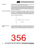
Reset Register
Programming Enable Register
Programming Command Register
Flash Data Byte Register
355
2549A–AVR–03/05

 ATMEL [ ATMEL ]