ATmega640/1280/1281/2560/2561
Some examples of UBRRn values for some system clock frequencies are found in Table
106 on page 227.
Double Speed Operation
(U2Xn)
The transfer rate can be doubled by setting the U2Xn bit in UCSRnA. Setting this bit
only has effect for the asynchronous operation. Set this bit to zero when using synchro-
nous operation.
Setting this bit will reduce the divisor of the baud rate divider from 16 to 8, effectively
doubling the transfer rate for asynchronous communication. Note however that the
Receiver will in this case only use half the number of samples (reduced from 16 to 8) for
data sampling and clock recovery, and therefore a more accurate baud rate setting and
system clock are required when this mode is used. For the Transmitter, there are no
downsides.
External Clock
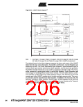
External clocking is used by the synchronous slave modes of operation. The description
in this section refers to Figure 84 for details.
External clock input from the XCKn pin is sampled by a synchronization register to mini-
mize the chance of meta-stability. The output from the synchronization register must
then pass through an edge detector before it can be used by the Transmitter and
Receiver. This process introduces a two CPU clock period delay and therefore the max-
imum external XCKn clock frequency is limited by the following equation:
f
OSC
-----------
f
<
XCK
4
Note that fosc depends on the stability of the system clock source. It is therefore recom-
mended to add some margin to avoid possible loss of data due to frequency variations.
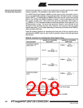
Synchronous Clock Operation When synchronous mode is used (UMSELn = 1), the XCKn pin will be used as either
clock input (Slave) or clock output (Master). The dependency between the clock edges
and data sampling or data change is the same. The basic principle is that data input (on
RxDn) is sampled at the opposite XCKn clock edge of the edge the data output (TxDn)
is changed.
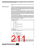
Figure 85. Synchronous Mode XCKn Timing.
UCPOL = 1
XCK
RxD / TxD
Sample
Sample
UCPOL = 0
XCK
RxD / TxD
The UCPOLn bit UCRSC selects which XCKn clock edge is used for data sampling and
which is used for data change. As Figure 85 shows, when UCPOLn is zero the data will
be changed at rising XCKn edge and sampled at falling XCKn edge. If UCPOLn is set,
the data will be changed at falling XCKn edge and sampled at rising XCKn edge.
209
2549A–AVR–03/05

 ATMEL [ ATMEL ]