ATmega640/1280/1281/2560/2561
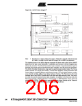
Clock Generation
The Clock Generation logic generates the base clock for the Transmitter and Receiver.
The USARTn supports four modes of clock operation: Normal asynchronous, Double
Speed asynchronous, Master synchronous and Slave synchronous mode. The UMSELn
bit in USART Control and Status Register C (UCSRnC) selects between asynchronous
and synchronous operation. Double Speed (asynchronous mode only) is controlled by
the U2Xn found in the UCSRnA Register. When using synchronous mode (UMSELn =
1), the Data Direction Register for the XCKn pin (DDR_XCKn) controls whether the
clock source is internal (Master mode) or external (Slave mode). The XCKn pin is only
active when using synchronous mode.
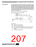
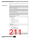
Figure 84 shows a block diagram of the clock generation logic.
Figure 84. Clock Generation Logic, Block Diagram
UBRR
U2X
fosc
UBRR+1
Prescaling
Down-Counter
/2
/4
/2
0
1
0
1
OSC
txclk
UMSEL
rxclk
DDR_XCK
Sync
Register
Edge
Detector
xcki
0
1
XCK
Pin
xcko
DDR_XCK
UCPOL
1
0
Signal description:
txclk Transmitter clock (Internal Signal).
rxclk Receiver base clock (Internal Signal).
xcki
Input from XCK pin (internal Signal). Used for synchronous slave operation.
xcko Clock output to XCK pin (Internal Signal). Used for synchronous master
operation.
fOSC
XTAL pin frequency (System Clock).
207
2549A–AVR–03/05

 ATMEL [ ATMEL ]