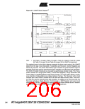
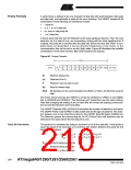
Figure 83. USART Block Diagram(1)
Clock Generator
UBRR[H:L]
OSC
BAUD RATE GENERATOR
SYNC LOGIC
PIN
CONTROL
XCK
TxD
RxD
Transmitter
TX
CONTROL
UDR (Transmit)
PARITY
GENERATOR
PIN
CONTROL
TRANSMIT SHIFT REGISTER
Receiver
CLOCK
RECOVERY
RX
CONTROL
DATA
RECOVERY
PIN
CONTROL
RECEIVE SHIFT REGISTER
PARITY
CHECKER
UDR (Receive)
UCSRA
UCSRB
UCSRC
Note:
1. See Figure 1 on page 2, Figure 2 on page 3, Table 45 on page 94, Table 48 on page
96, Table 57 on page 104 and Table 60 on page 106 for USART pin placement.
The dashed boxes in the block diagram separate the three main parts of the USART
(listed from the top): Clock Generator, Transmitter and Receiver. Control Registers are
shared by all units. The Clock Generation logic consists of synchronization logic for
external clock input used by synchronous slave operation, and the baud rate generator.
The XCKn (Transfer Clock) pin is only used by synchronous transfer mode. The Trans-
mitter consists of a single write buffer, a serial Shift Register, Parity Generator and
Control logic for handling different serial frame formats. The write buffer allows a contin-
uous transfer of data without any delay between frames. The Receiver is the most
complex part of the USART module due to its clock and data recovery units. The recov-
ery units are used for asynchronous data reception. In addition to the recovery units, the
Receiver includes a Parity Checker, Control logic, a Shift Register and a two level
receive buffer (UDRn). The Receiver supports the same frame formats as the Transmit-
ter, and can detect Frame Error, Data OverRun and Parity Errors.
206
ATmega640/1280/1281/2560/2561
2549A–AVR–03/05

 ATMEL [ ATMEL ]