ATmega640/1280/1281/2560/2561
Be aware that the COM2x1:0 bits are not double buffered together with the compare
value. Changing the COM2x1:0 bits will take effect immediately.
Compare Match Output
Unit
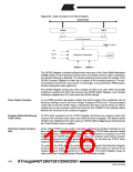
The Compare Output mode (COM2x1:0) bits have two functions. The Waveform Gener-
ator uses the COM2x1:0 bits for defining the Output Compare (OC2x) state at the next
compare match. Also, the COM2x1:0 bits control the OC2x pin output source. Figure 70
shows a simplified schematic of the logic affected by the COM2x1:0 bit setting. The I/O
Registers, I/O bits, and I/O pins in the figure are shown in bold. Only the parts of the
general I/O Port Control Registers (DDR and PORT) that are affected by the COM2x1:0
bits are shown. When referring to the OC2x state, the reference is for the internal OC2x
Register, not the OC2x pin.
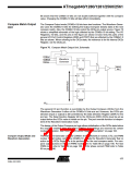
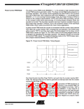
Figure 70. Compare Match Output Unit, Schematic
COMnx1
Waveform
Generator
COMnx0
FOCnx
D
Q
1
0
OCnx
Pin
OCnx
D
Q
PORT
D
Q
DDR
clkI/O
The general I/O port function is overridden by the Output Compare (OC2x) from the
Waveform Generator if either of the COM2x1:0 bits are set. However, the OC2x pin
direction (input or output) is still controlled by the Data Direction Register (DDR) for the
port pin. The Data Direction Register bit for the OC2x pin (DDR_OC2x) must be set as
output before the OC2x value is visible on the pin. The port override function is indepen-
dent of the Waveform Generation mode.
The design of the Output Compare pin logic allows initialization of the OC2x state before
the output is enabled. Note that some COM2x1:0 bit settings are reserved for certain
modes of operation. See “8-bit Timer/Counter Register Description” on page 184.
Compare Output Mode and
Waveform Generation
The Waveform Generator uses the COM2x1:0 bits differently in normal, CTC, and PWM
modes. For all modes, setting the COM2x1:0 = 0 tells the Waveform Generator that no
action on the OC2x Register is to be performed on the next compare match. For com-
pare output actions in the non-PWM modes refer to Table 88 on page 185. For fast
PWM mode, refer to Table 89 on page 185, and for phase correct PWM refer to Table
90 on page 186.
177
2549A–AVR–03/05

 ATMEL [ ATMEL ]