ATmega640/1280/1281/2560/2561
used for updating the TOP value. However, changing TOP to a value close to BOTTOM
when the counter is running with none or a low prescaler value must be done with care
since the CTC mode does not have the double buffering feature. If the new value written
to OCR2A is lower than the current value of TCNT2, the counter will miss the compare
match. The counter will then have to count to its maximum value (0xFF) and wrap
around starting at 0x00 before the compare match can occur.
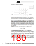
For generating a waveform output in CTC mode, the OC2A output can be set to toggle
its logical level on each compare match by setting the Compare Output mode bits to tog-
gle mode (COM2A1:0 = 1). The OC2A value will not be visible on the port pin unless the
data direction for the pin is set to output. The waveform generated will have a maximum
frequency of fOC2A = fclk_I/O/2 when OCR2A is set to zero (0x00). The waveform fre-
quency is defined by the following equation:
f
clk_I/O
f
= -------------------------------------------------
OCnx
2 ⋅ N ⋅ (1 + OCRnx)
The N variable represents the prescale factor (1, 8, 32, 64, 128, 256, or 1024).
As for the Normal mode of operation, the TOV2 Flag is set in the same timer clock cycle
that the counter counts from MAX to 0x00.
Fast PWM Mode
The fast Pulse Width Modulation or fast PWM mode (WGM22:0 = 3 or 7) provides a high
frequency PWM waveform generation option. The fast PWM differs from the other PWM
option by its single-slope operation. The counter counts from BOTTOM to TOP then
restarts from BOTTOM. TOP is defined as 0xFF when WGM22:0 = 3, and OCR2A when
MGM22:0 = 7. In non-inverting Compare Output mode, the Output Compare (OC2x) is
cleared on the compare match between TCNT2 and OCR2x, and set at BOTTOM. In
inverting Compare Output mode, the output is set on compare match and cleared at
BOTTOM. Due to the single-slope operation, the operating frequency of the fast PWM
mode can be twice as high as the phase correct PWM mode that uses dual-slope oper-
ation. This high frequency makes the fast PWM mode well suited for power regulation,
rectification, and DAC applications. High frequency allows physically small sized exter-
nal components (coils, capacitors), and therefore reduces total system cost.
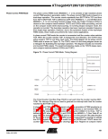
In fast PWM mode, the counter is incremented until the counter value matches the TOP
value. The counter is then cleared at the following timer clock cycle. The timing diagram
for the fast PWM mode is shown in Figure 61. The TCNT2 value is in the timing diagram
shown as a histogram for illustrating the single-slope operation. The diagram includes
non-inverted and inverted PWM outputs. The small horizontal line marks on the TCNT2
slopes represent compare matches between OCR2x and TCNT2.
179
2549A–AVR–03/05

 ATMEL [ ATMEL ]