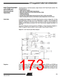
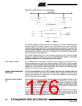
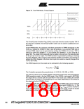
Figure 69. Output Compare Unit, Block Diagram
DATA BUS
OCRnx
TCNTn
=
(8-bit Comparator )
OCFnx (Int.Req.)
top
bottom
FOCn
Waveform Generator
OCnx
WGMn1:0
COMnX1:0
The OCR2x Register is double buffered when using any of the Pulse Width Modulation
(PWM) modes. For the Normal and Clear Timer on Compare (CTC) modes of operation,
the double buffering is disabled. The double buffering synchronizes the update of the
OCR2x Compare Register to either top or bottom of the counting sequence. The syn-
chronization prevents the occurrence of odd-length, non-symmetrical PWM pulses,
thereby making the output glitch-free.
The OCR2x Register access may seem complex, but this is not case. When the double
buffering is enabled, the CPU has access to the OCR2x Buffer Register, and if double
buffering is disabled the CPU will access the OCR2x directly.
Force Output Compare
In non-PWM waveform generation modes, the match output of the comparator can be
forced by writing a one to the Force Output Compare (FOC2x) bit. Forcing compare
match will not set the OCF2x Flag or reload/clear the timer, but the OC2x pin will be
updated as if a real compare match had occurred (the COM2x1:0 bits settings define
whether the OC2x pin is set, cleared or toggled).
Compare Match Blocking by
TCNT2 Write
All CPU write operations to the TCNT2 Register will block any compare match that
occurs in the next timer clock cycle, even when the timer is stopped. This feature allows
OCR2x to be initialized to the same value as TCNT2 without triggering an interrupt when
the Timer/Counter clock is enabled.
Using the Output Compare
Unit
Since writing TCNT2 in any mode of operation will block all compare matches for one
timer clock cycle, there are risks involved when changing TCNT2 when using the Output
Compare channel, independently of whether the Timer/Counter is running or not. If the
value written to TCNT2 equals the OCR2x value, the compare match will be missed,
resulting in incorrect waveform generation. Similarly, do not write the TCNT2 value
equal to BOTTOM when the counter is downcounting.
The setup of the OC2x should be performed before setting the Data Direction Register
for the port pin to output. The easiest way of setting the OC2x value is to use the Force
Output Compare (FOC2x) strobe bit in Normal mode. The OC2x Register keeps its
value even when changing between Waveform Generation modes.
176
ATmega640/1280/1281/2560/2561
2549A–AVR–03/05

 ATMEL [ ATMEL ]