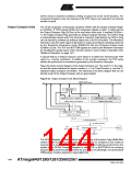
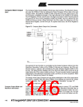
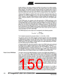
Compare Match Output
Unit
The Compare Output mode (COMnx1:0) bits have two functions. The Waveform Gener-
ator uses the COMnx1:0 bits for defining the Output Compare (OCnx) state at the next
compare match. Secondly the COMnx1:0 bits control the OCnx pin output source. Fig-
ure 53 shows a simplified schematic of the logic affected by the COMnx1:0 bit setting.
The I/O Registers, I/O bits, and I/O pins in the figure are shown in bold. Only the parts of
the general I/O Port Control Registers (DDR and PORT) that are affected by the
COMnx1:0 bits are shown. When referring to the OCnx state, the reference is for the
internal OCnx Register, not the OCnx pin. If a system reset occur, the OCnx Register is
reset to “0”.
Figure 53. Compare Match Output Unit, Schematic
COMnx1
Waveform
Generator
COMnx0
FOCnx
D
Q
1
0
OCnx
Pin
OCnx
D
Q
PORT
D
Q
DDR
clkI/O
The general I/O port function is overridden by the Output Compare (OCnx) from the
Waveform Generator if either of the COMnx1:0 bits are set. However, the OCnx pin
direction (input or output) is still controlled by the Data Direction Register (DDR) for the
port pin. The Data Direction Register bit for the OCnx pin (DDR_OCnx) must be set as
output before the OCnx value is visible on the pin. The port override function is generally
independent of the Waveform Generation mode, but there are some exceptions. Refer
to Table 79, Table 80 and Table 81 for details.
The design of the Output Compare pin logic allows initialization of the OCnx state before
the output is enabled. Note that some COMnx1:0 bit settings are reserved for certain
modes of operation. See “16-bit Timer/Counter Register Description” on page 157.
The COMnx1:0 bits have no effect on the Input Capture unit.
Compare Output Mode and
Waveform Generation
The Waveform Generator uses the COMnx1:0 bits differently in normal, CTC, and PWM
modes. For all modes, setting the COMnx1:0 = 0 tells the Waveform Generator that no
action on the OCnx Register is to be performed on the next compare match. For com-
pare output actions in the non-PWM modes refer to Table 79 on page 158. For fast
PWM mode refer to Table 80 on page 158, and for phase correct and phase and fre-
quency correct PWM refer to Table 81 on page 159.
146
ATmega640/1280/1281/2560/2561
2549A–AVR–03/05

 ATMEL [ ATMEL ]