(ICFn) must be cleared by software (writing a logical one to the I/O bit location). For
measuring frequency only, the clearing of the ICFn Flag is not required (if an interrupt
handler is used).
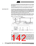
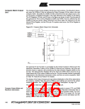
Output Compare Units
The 16-bit comparator continuously compares TCNTn with the Output Compare Regis-
ter (OCRnx). If TCNT equals OCRnx the comparator signals a match. A match will set
the Output Compare Flag (OCFnx) at the next timer clock cycle. If enabled (OCIEnx =
1), the Output Compare Flag generates an Output Compare interrupt. The OCFnx Flag
is automatically cleared when the interrupt is executed. Alternatively the OCFnx Flag
can be cleared by software by writing a logical one to its I/O bit location. The Waveform
Generator uses the match signal to generate an output according to operating mode set
by the Waveform Generation mode (WGMn3:0) bits and Compare Output mode
(COMnx1:0) bits. The TOP and BOTTOM signals are used by the Waveform Generator
for handling the special cases of the extreme values in some modes of operation (See
“Modes of Operation” on page 147.)
A special feature of Output Compare unit A allows it to define the Timer/Counter TOP
value (i.e., counter resolution). In addition to the counter resolution, the TOP value
defines the period time for waveforms generated by the Waveform Generator.
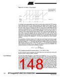
Figure 52 shows a block diagram of the Output Compare unit. The small “n” in the regis-
ter and bit names indicates the device number (n = n for Timer/Counter n), and the “x”
indicates Output Compare unit (A/B/C). The elements of the block diagram that are not
directly a part of the Output Compare unit are gray shaded.
Figure 52. Output Compare Unit, Block Diagram
DATA BUS (8-bit)
TEMP (8-bit)
OCRnxH Buf. (8-bit)
OCRnxL Buf. (8-bit)
TCNTnH (8-bit)
TCNTnL (8-bit)
OCRnx Buffer (16-bit Register)
TCNTn (16-bit Counter)
OCRnxH (8-bit)
OCRnxL (8-bit)
OCRnx (16-bit Register)
= (16-bit Comparator )
OCFnx (Int.Req.)
TOP
OCnx
Waveform Generator
BOTTOM
WGMn3:0
COMnx1:0
The OCRnx Register is double buffered when using any of the twelve Pulse Width Mod-
ulation (PWM) modes. For the Normal and Clear Timer on Compare (CTC) modes of
operation, the double buffering is disabled. The double buffering synchronizes the
update of the OCRnx Compare Register to either TOP or BOTTOM of the counting
sequence. The synchronization prevents the occurrence of odd-length, non-symmetrical
PWM pulses, thereby making the output glitch-free.
144
ATmega640/1280/1281/2560/2561
2549A–AVR–03/05

 ATMEL [ ATMEL ]