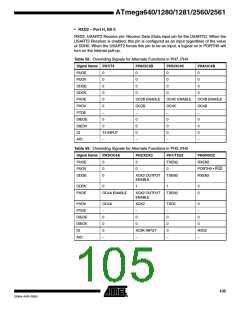
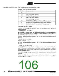
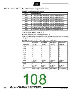
Alternate Functions of Port J
The Port J alternate pin configuration is as follows:
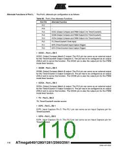
Table 60. Port J Pins Alternate Functions
Port Pin
PJ7
Alternate Function
–
PJ6
PCINT15 (Pin Change Interrupt 15)
PJ5
PCINT14 (Pin Change Interrupt 14)
PJ4
PCINT13 (Pin Change Interrupt 13)
PJ3
PCINT12 (Pin Change Interrupt 12)
PJ2
XCK3/PCINT11 (USART3 External Clock or Pin Change Interrupt 11)
TXD3/PCINT10 (USART3 Transmit Pin or Pin Change Interrupt 10)
RXD3/PCINT9 (USART3 Receive Pin or Pin Change Interrupt 9)
PJ1
PJ0
• PCINT15:12 - Port J, Bit 6:3
PCINT15:12, Pin Change Interrupt Source 15:12. The PJ6:3 pins can serve as External
Interrupt Sources
• XCK2/PCINT11 - Port J, Bit 2
XCK2, USART 2 External Clock. The Data Direction Register (DDJ2) controls whether
the clock is output (DDJ2 set) or input (DDJ2 cleared). The XCK2 pin is active only when
the USART2 operates in synchronous mode.
PCINT11, Pin Change Interrupt Source 11. The PJ2 pins can serve as External Interrupt
Sources
• TXD3/PCINT10 - Port J, Bit 1
TXD3, USART3 Transmit pin
PCINT10, Pin Change Interrupt Source 10. The PJ2 pins can serve as External Interrupt
Sources
• RXD3/PCINT9 - Port J, Bit 0
RXD3, USART3 Receive pin. Receive Data (Data input pin for the USART3). When the
USART3 Receiver is enabled, this pin is configured as an input regardless of the value
of DDJ0. When the USART3 forces this pin to be an input, a logical one in PORTJ0 will
turn on the internal pull-up.
PCINT9, Pin Change Interrupt Source 9. The PJ2 pins can serve as External Interrupt
Sources
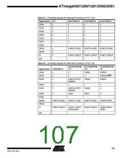
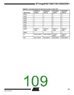
Table 61 and Table 62 relates the alternate functions of Port J to the overriding signals
shown in Figure 37 on page 86
106
ATmega640/1280/1281/2560/2561
2549A–AVR–03/05

 ATMEL [ ATMEL ]