Alternate Functions of Port H The Port H alternate pin configuration is as follows:
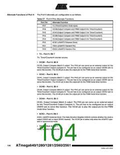
Table 57. Port H Pins Alternate Functions
Port Pin
PH7
Alternate Function
T4 (Timer/Counter4 Clock Input)
PH6
OC2B(Output Compare and PWM Output B for Timer/Counter2)
OC4C(Output Compare and PWM Output C for Timer/Counter4)
OC4B(Output Compare and PWM Output B for Timer/Counter4)
OC4A(Output Compare and PWM Output A for Timer/Counter4)
XCK2 (USART2 External Clock)
PH5
PH4
PH3
PH2
PH1
TXD2 (USART2 Transmit Pin)
PH0
RXD2 (USART2 Receive Pin)
• T4 – Port H, Bit 7
T4, Timer/Counter4 counter source.
• OC2B – Port H, Bit 6
OC2B, Output Compare Match B output: The PH6 pin can serve as an external output for the
Timer/Counter2 Output Compare B. The pin has to be configured as an output (DDH6 set) to
serve this function. The OC2B pin is also the output pin for the PWM mode timer function.
• OC4C – Port H, Bit 5
OC4C, Output Compare Match C output: The PH5 pin can serve as an external output for the
Timer/Counter4 Output Compare C. The pin has to be configured as an output (DDH5 set) to
serve this function. The OC4C pin is also the output pin for the PWM mode timer function.
• OC4B – Port H, Bit 4
OC4B, Output Compare Match B output: The PH4 pin can serve as an external output for the
Timer/Counter2 Output Compare B. The pin has to be configured as an output (DDH4 set) to
serve this function. The OC4B pin is also the output pin for the PWM mode timer function.
• OC4A – Port H, Bit 3
OC4C, Output Compare Match A output: The PH3 pin can serve as an external output
for the Timer/Counter4 Output Compare A. The pin has to be configured as an output
(DDH3 set) to serve this function. The OC4A pin is also the output pin for the PWM
mode timer function.
• XCK2 – Port H, Bit 2
XCK2, USART2 External Clock: The Data Direction Register (DDH2) controls whether the clock is
output (DDH2 set) or input (DDH2 cleared). The XC2K pin is active only when the USART2 oper-
ates in synchronous mode.
• TXD2 – Port H, Bit 1
TXD2, USART2 Transmit Pin.
104
ATmega640/1280/1281/2560/2561
2549A–AVR–03/05

 ATMEL [ ATMEL ]