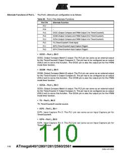
Alternate Functions of Port L
The Port L alternate pin configuration is as follows:
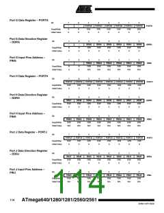
Table 66. Port L Pins Alternate Functions
Port Pin
PL7
Alternate Function
–
PL6
–
PL5
OC5C (Output Compare and PWM Output C for Timer/Counter5)
OC5B (Output Compare and PWM Output B for Timer/Counter5)
OC5A (Output Compare and PWM Output A for Timer/Counter5)
T5 (Timer/Counter5 Clock Input)
PL4
PL3
PL2
PL1
ICP5 (Timer/Counter5 Input Capture Trigger)
ICP4 (Timer/Counter4 Input Capture Trigger)
PL0
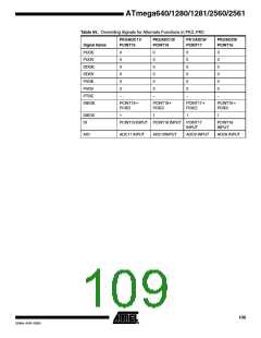
• OC5C – Port L, Bit 5
OC5C, Output Compare Match C output: The PL5 pin can serve as an external output
for the Timer/Counter5 Output Compare C. The pin has to be configured as an output
(DDL5 set) to serve this function. The OC5C pin is also the output pin for the PWM
mode timer function.
• OC5B – Port L, Bit 4
OC5B, Output Compare Match B output: The PL4 pin can serve as an external output
for the Timer/Counter 5 Output Compare B. The pin has to be configured as an output
(DDL4 set) to serve this function. The OC5B pin is also the output pin for the PWM
mode timer function.
• OC5A – Port L, Bit 3
OC5A, Output Compare Match A output: The PL3 pin can serve as an external output
for the Timer/Counter 5 Output Compare A. The pin has to be configured as an output
(DDL3 set) to serve this function. The OC5A pin is also the output pin for the PWM
mode timer function.
• T5 – Port L, Bit 2
T5, Timer/Counter5 counter source.
• ICP5 – Port L, Bit 1
ICP5, Input Capture Pin 5: The PL1 pin can serve as an Input Capture pin for
Timer/Counter5.
• ICP4 – Port L, Bit 0
ICP4, Input Capture Pin 4: The PL0 pin can serve as an Input Capture pin for
Timer/Counter4.
110
ATmega640/1280/1281/2560/2561
2549A–AVR–03/05

 ATMEL [ ATMEL ]