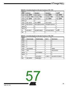
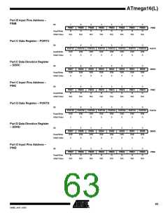
ATmega16(L)
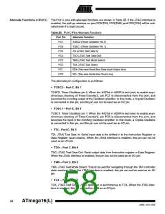
• OC1A – Port D, Bit 5
OC1A, Output Compare Match A output: The PD5 pin can serve as an external output
for the Timer/Counter1 Output Compare A. The pin has to be configured as an output
(DDD5 set (one)) to serve this function. The OC1A pin is also the output pin for the
PWM mode timer function.
• OC1B – Port D, Bit 4
OC1B, Output Compare Match B output: The PD4 pin can serve as an external output
for the Timer/Counter1 Output Compare B. The pin has to be configured as an output
(DDD4 set (one)) to serve this function. The OC1B pin is also the output pin for the
PWM mode timer function.
• INT1 – Port D, Bit 3
INT1, External Interrupt Source 1: The PD3 pin can serve as an external interrupt
source.
• INT0 – Port D, Bit 2
INT0, External Interrupt Source 0: The PD2 pin can serve as an external interrupt
source.
• TXD – Port D, Bit 1
TXD, Transmit Data (Data output pin for the USART). When the USART Transmitter is
enabled, this pin is configured as an output regardless of the value of DDD1.
• RXD – Port D, Bit 0
RXD, Receive Data (Data input pin for the USART). When the USART Receiver is
enabled this pin is configured as an input regardless of the value of DDD0. When the
USART forces this pin to be an input, the pull-up can still be controlled by the PORTD0
bit.
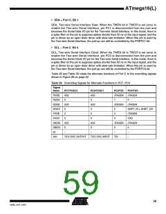
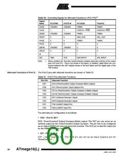
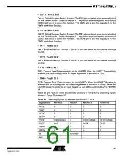
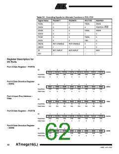
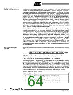
Table 32 and Table 33 relate the alternate functions of Port D to the overriding signals
shown in Figure 26 on page 52.
Table 32. Overriding Signals for Alternate Functions PD7..PD4
Signal Name
PUOE
PUOV
DDOE
DDOV
PVOE
PVOV
DIEOE
DIEOV
DI
PD7/OC2
PD6/ICP
PD5/OC1A
PD4/OC1B
0
0
0
0
0
0
0
0
0
0
0
0
0
0
0
0
OC2 ENABLE
0
OC1A ENABLE
OC1B ENABLE
OC2
0
OC1A
OC1B
0
0
–
–
0
0
0
–
–
0
0
–
–
0
ICP INPUT
–
AIO
61
2466E–AVR–10/02

 ATMEL [ ATMEL ]