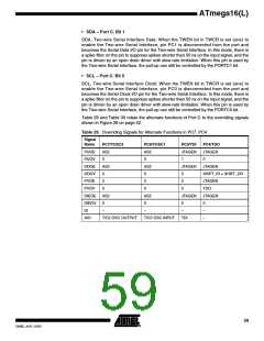
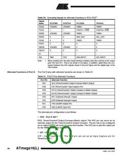
Table 30. Overriding Signals for Alternate Functions in PC3..PC0(1)
Signal
Name
PUOE
PUOV
DDOE
DDOV
PVOE
PVOV
DIEOE
DIEOV
DI
PC3/TMS
PC2/TCK
PC1/SDA
PC0/SCL
JTAGEN
JTAGEN
TWEN
TWEN
1
1
PORTC1 • PUD
PORTC0 • PUD
JTAGEN
JTAGEN
TWEN
TWEN
0
0
SDA_OUT
SCL_OUT
0
0
TWEN
TWEN
0
0
0
0
JTAGEN
JTAGEN
0
0
0
0
0
0
–
–
–
–
AIO
TMS
TCK
SDA INPUT
SCL INPUT
Note:
1. When enabled, the Two-wire Serial Interface enables slew-rate controls on the output
pins PC0 and PC1. This is not shown in the figure. In addition, spike filters are con-
nected between the AIO outputs shown in the port figure and the digital logic of the
TWI module.
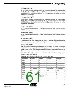
Alternate Functions of Port D The Port D pins with alternate functions are shown in Table 31.
Table 31. Port D Pins Alternate Functions
Port Pin
PD7
Alternate Function
OC2 (Timer/Counter2 Output Compare Match Output)
ICP (Timer/Counter1 Input Capture Pin)
OC1A (Timer/Counter1 Output Compare A Match Output)
OC1B (Timer/Counter1 Output Compare B Match Output)
INT1 (External Interrupt 1 Input)
PD6
PD5
PD4
PD3
PD2
INT0 (External Interrupt 0 Input)
PD1
TXD (USART Output Pin)
PD0
RXD (USART Input Pin)
The alternate pin configuration is as follows:
• OC2 – Port D, Bit 7
OC2, Timer/Counter2 Output Compare Match output: The PD7 pin can serve as an
external output for the Timer/Counter2 Output Compare. The pin has to be configured
as an output (DDD7 set (one)) to serve this function. The OC2 pin is also the output pin
for the PWM mode timer function.
• ICP – Port D, Bit 6
ICP – Input Capture Pin: The PD6 pin can act as an Input Capture pin for
Timer/Counter1.
60
ATmega16(L)
2466E–AVR–10/02

 ATMEL [ ATMEL ]