ATmega16(L)
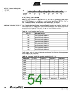
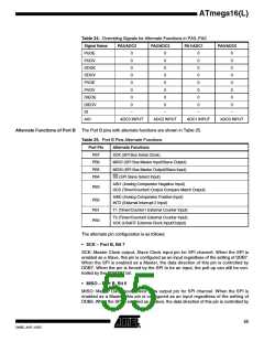
Table 24. Overriding Signals for Alternate Functions in PA3..PA0
Signal Name
PUOE
PUOV
DDOE
DDOV
PVOE
PVOV
DIEOE
DIEOV
DI
PA3/ADC3
PA2/ADC2
PA1/ADC1
PA0/ADC0
0
0
0
0
0
0
0
0
0
0
0
0
0
0
0
0
0
0
0
0
0
0
0
0
0
0
0
0
0
0
0
0
–
–
–
–
AIO
ADC3 INPUT
ADC2 INPUT
ADC1 INPUT
ADC0 INPUT
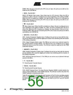
Alternate Functions of Port B The Port B pins with alternate functions are shown in Table 25.
Table 25. Port B Pins Alternate Functions
Port Pin
PB7
Alternate Functions
SCK (SPI Bus Serial Clock)
PB6
MISO (SPI Bus Master Input/Slave Output)
MOSI (SPI Bus Master Output/Slave Input)
SS (SPI Slave Select Input)
PB5
PB4
AIN1 (Analog Comparator Negative Input)
PB3
OC0 (Timer/Counter0 Output Compare Match Output)
AIN0 (Analog Comparator Positive Input)
INT2 (External Interrupt 2 Input)
PB2
PB1
PB0
T1 (Timer/Counter1 External Counter Input)
T0 (Timer/Counter0 External Counter Input)
XCK (USART External Clock Input/Output)
The alternate pin configuration is as follows:
• SCK – Port B, Bit 7
SCK: Master Clock output, Slave Clock input pin for SPI channel. When the SPI is
enabled as a Slave, this pin is configured as an input regardless of the setting of DDB7.
When the SPI is enabled as a Master, the data direction of this pin is controlled by
DDB7. When the pin is forced by the SPI to be an input, the pull-up can still be con-
trolled by the PORTB7 bit.
• MISO – Port B, Bit 6
MISO: Master Data input, Slave Data output pin for SPI channel. When the SPI is
enabled as a Master, this pin is configured as an input regardless of the setting of
DDB6. When the SPI is enabled as a Slave, the data direction of this pin is controlled by
55
2466E–AVR–10/02

 ATMEL [ ATMEL ]